Group II-VI semiconductor devices

Inactive Publication Date: 2007-06-05
ZENO MATERIALS LLC
View PDF17 Cites 48 Cited by
  • Summary
  • Abstract
  • Description
  • Claims
  • Application Information

AI Technical Summary

Benefits of technology

[0007]The present invention is drawn to semiconductor devices that contain group II-VI semiconductor materials. The devices may include a p-n junction containing a p-type group II-VI semiconductor material and an n-type semiconductor material. The p-type group II-VI semiconductor includes single crystal group II-VI semiconductors containing atoms of group II elements,

Problems solved by technology

P-type zinc oxide semiconductor materials are theoretically possible, but have been difficult to prepare.
Their stability has been questioned.
Some of the more-stable p-type zinc oxide materials reporte

Method used


Image

  • Group II-VI semiconductor devices
  • Group II-VI semiconductor devices
  • Group II-VI semiconductor devices

Examples


example 1

Sputtering of ZnO with Arsenic as a Dopant

[0067]A thin film of p-type zinc oxide was deposited onto a self supporting substrate by RF sputtering. Both fused silica and silicon wafers were used as the self supporting substrate. The sputtering target composition was ZnO (0.99-0.95 moles)+As (0.01-0.05 moles). The preferred target composition was ZnO (0.98 moles)+As (0.02 moles). The substrate temperature was between 350 and 550° C. The preferred temperature was about 400° C. The RF power was between 20 and 120 watts. The preferred power was about 60 watts. The sputtering atmosphere included argon at a gas pressure of about 4 to 20 mtorr and O2 at a gas pressure of about 1 to 4 mtorr. The preferred sputtering atmosphere pressures were about 9 mtorr argon and about 1 mtorr O2.

[0068]The resulting transparent p-type zinc oxide layer had a resistance of about 10,000 ohms / square. After annealing at 440° C. in air, the resistance dropped to about 1,000 ohms / square. In another composition pre...

example 2

Sputtering of ZnO with Arsenic as a Dopant

[0069]A thin film of p-type zinc oxide was deposited onto a self supporting substrate by RF sputtering. Both fused silica and silicon wafers were used as the self supporting substrate. The sputtering target composition was ZnO (0.99-0.95 moles)+As (0.01-0.05 moles). The preferred target composition was ZnO (0.98 moles)+As (0.02 moles). The substrate temperature was between 350 and 550° C. The preferred temperature was about 400° C. The RF power was between 20 and 120 watts. The preferred power was about 60 watts. The sputtering atmosphere included argon at a gas pressure of about 4 to 20 mtorr and H2 at a gas pressure of about 1 to 4 mtorr. The preferred sputtering atmosphere pressures were about 9 mtorr argon and about 1 mtorr H2.

[0070]The resulting transparent p-type zinc oxide layer had a resistance of about 500 ohms / square. Without being bound by theory, it is believed that the hydrogen gas may be moderating the concentration of oxygen i...

example 3

Sputtering of ZnO with Arsenic as a Dopant

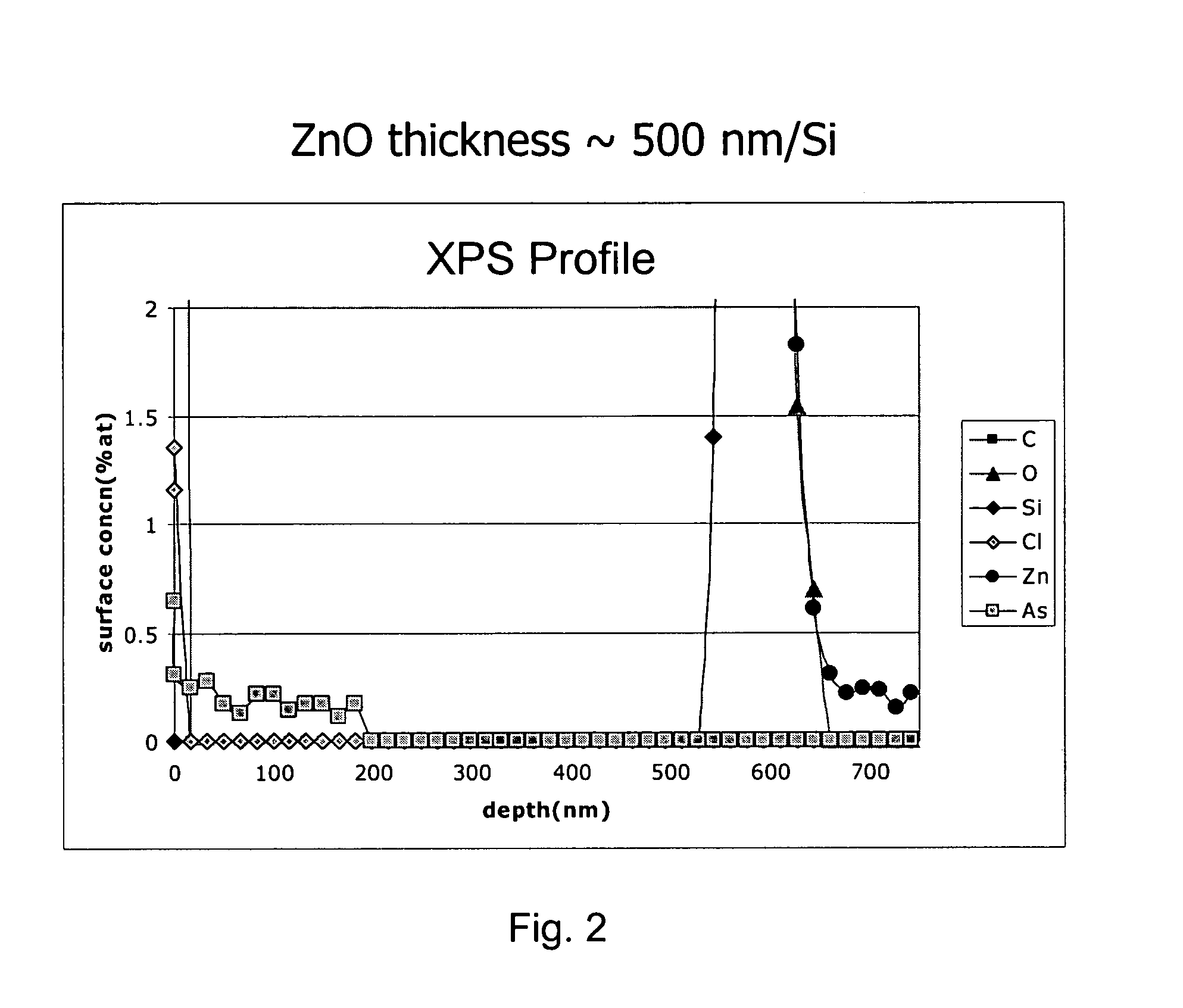
[0071]A thin film of p-type zinc oxide was deposited onto a self supporting substrate by RF sputtering. Both fused silica and silicon wafers were used as the self supporting substrate. The sputtering target composition was ZnO (0.99-0.95 moles)+As (0.01-0.05 moles). The preferred target composition was ZnO (0.975 moles)+As (0.025 moles). The substrate temperature was between 350 and 550° C. The preferred temperature was about 400° C. The RF power was between 20 and 120 watts. The preferred power was about 60 to 90 watts. The sputtering atmosphere included argon at a gas pressure of about 4 to 20 mtorr. The preferred sputtering atmosphere pressure was about 9 mtorr argon.

[0072]The resulting transparent p-type zinc oxide layer had a resistance of about 1000 ohms / square. The resulting p-type zinc oxide was analyzed by X-ray Photoelectron Spectroscopy (XPS). A graph of the XPS data is shown in FIG. 2. The data from FIG. 2 show arsenic in zinc ox...


PUM


Abstract

Semiconductor devices containing group II-VI semiconductor materials are disclosed. The devices may include a p-n junction containing a p-type group II-VI semiconductor material and an n-type semiconductor material. The p-type group II-VI semiconductor includes a single crystal group II-VI semiconductor containing atoms of group II elements, atoms of group VI elements, and one or more p-type dopants. The p-type dopant concentration is greater than about 1016 atoms·cm−3, the semiconductor resistivity is less than about 0.5 ohm·cm, and the carrier mobility is greater than about 0.1 cm2/V·s. The semiconductor devices may include light emitting diodes, laser diodes, field effect transistors, and photodetectors.

Description

CROSS-REFERENCE TO RELATED APPLICATIONS[0001]This application claims the benefit of U.S. Provisional Application No. 60 / 471,916, filed May 20, 2003, U.S. Provisional Application No. 60 / 488,677, filed Jul. 18, 2003, and U.S. Provisional Application No. 60 / 560,779, filed Apr. 8, 2004, which applications are incorporated by reference.BACKGROUND OF THE INVENTION[0002]The present invention provides group II-VI semiconductor devices and methods of fabrication.[0003]As used herein, the group II-VI semiconductor devices include devices fabricated from group II-VI semiconductor compounds which include group II elements selected from zinc, cadmium, the alkaline earth metals such as beryllium, magnesium calcium, strontium, and barium, and mixtures thereof, and group VI elements selected from oxygen, sulfur, selenium, tellurium, and mixtures thereof. The group II-VI semiconductor compounds may be doped with one or more p-type dopant. Such p-type dopants include, but are not limited to, nitrogen...

Claims


Application Information

Patent Timeline
IPC IPC(8): H01L33/00H01L21/365H01L21/368H01L29/22H01L29/267H01L33/28H01S5/30H01S5/327
CPCH01L21/0237H01L21/02554H01L21/02557H01L21/02565H01L21/02576H01L21/02579H01L21/02628H01L21/02631H01L29/22H01L29/267H01L33/285H01S5/327H01S5/3059
Inventor BURGENER, II, ROBERT H.FELIX, ROGER L.RENLUND, GARY M.
Owner ZENO MATERIALS LLC
Why Eureka
Try Eureka