Patterning of devices

a technology of devices and printed circuits, applied in the field of devices, can solve the problems of inability to directly apply thermal printing technologies to the fabrication of electroactive transistor circuits, incompatibility of exposure temperatures used in thermal imagers with the fabrication of polymer transistor circuits, and significantly more difficult fabrication of active electronic circuits than printing plates, so as to achieve the effect of improving printing speed

Inactive Publication Date: 2007-07-17
ETV CAPITAL
View PDF11 Cites 41 Cited by
  • Summary
  • Abstract
  • Description
  • Claims
  • Application Information

AI Technical Summary

Benefits of technology

[0011]A typical platesetter for direct laser imaging consists of a linear array of individually controlled laser diodes 5, 5′, 5″ coupled to optical fibres 25, and focussed onto the surface of the printing plate using a telecentric lens system 4 (FIG. 10(a)). Alternatively, an unfocussed laser source 5 coupled to a cylindrical lens asse...

Problems solved by technology

It is clear from the above description that direct application of thermal printing technologies to the fabrication of electroactive transistor circuits is not possible.
The exposure temperatures used in thermal imagers are not compatible with the fabricati...

Method used


Image

  • Patterning of devices
  • Patterning of devices
  • Patterning of devices

Examples


Embodiment Construction

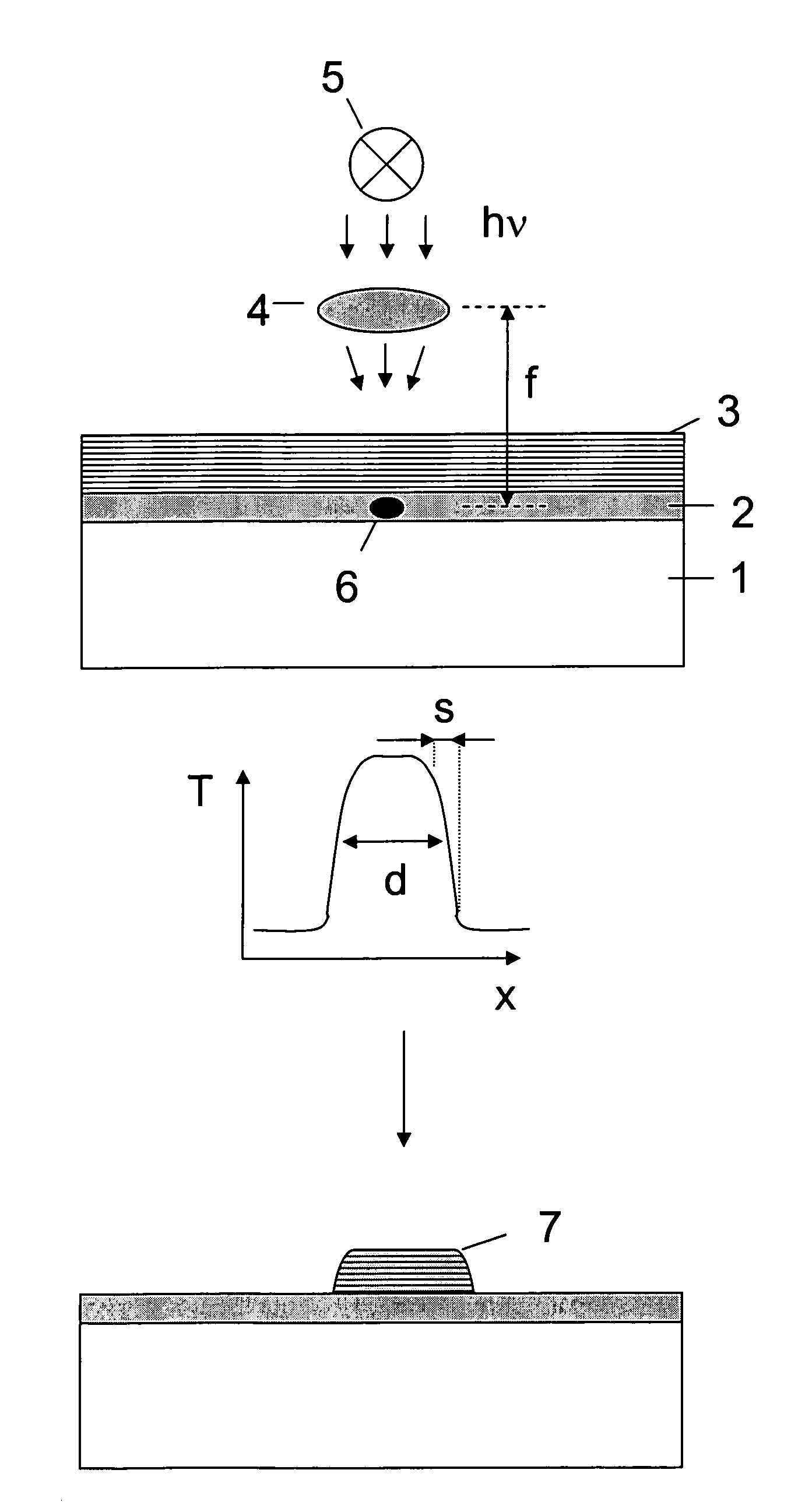
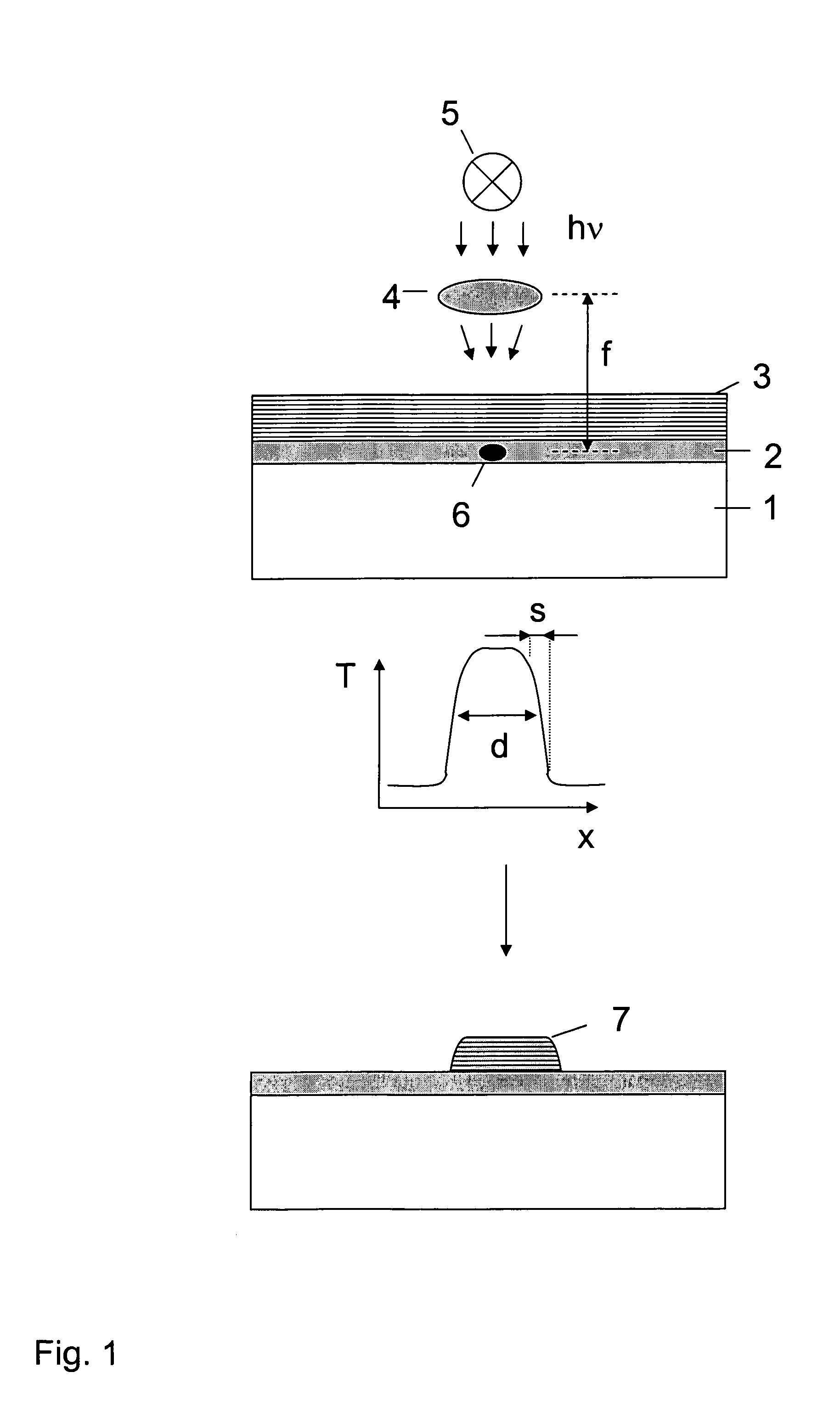
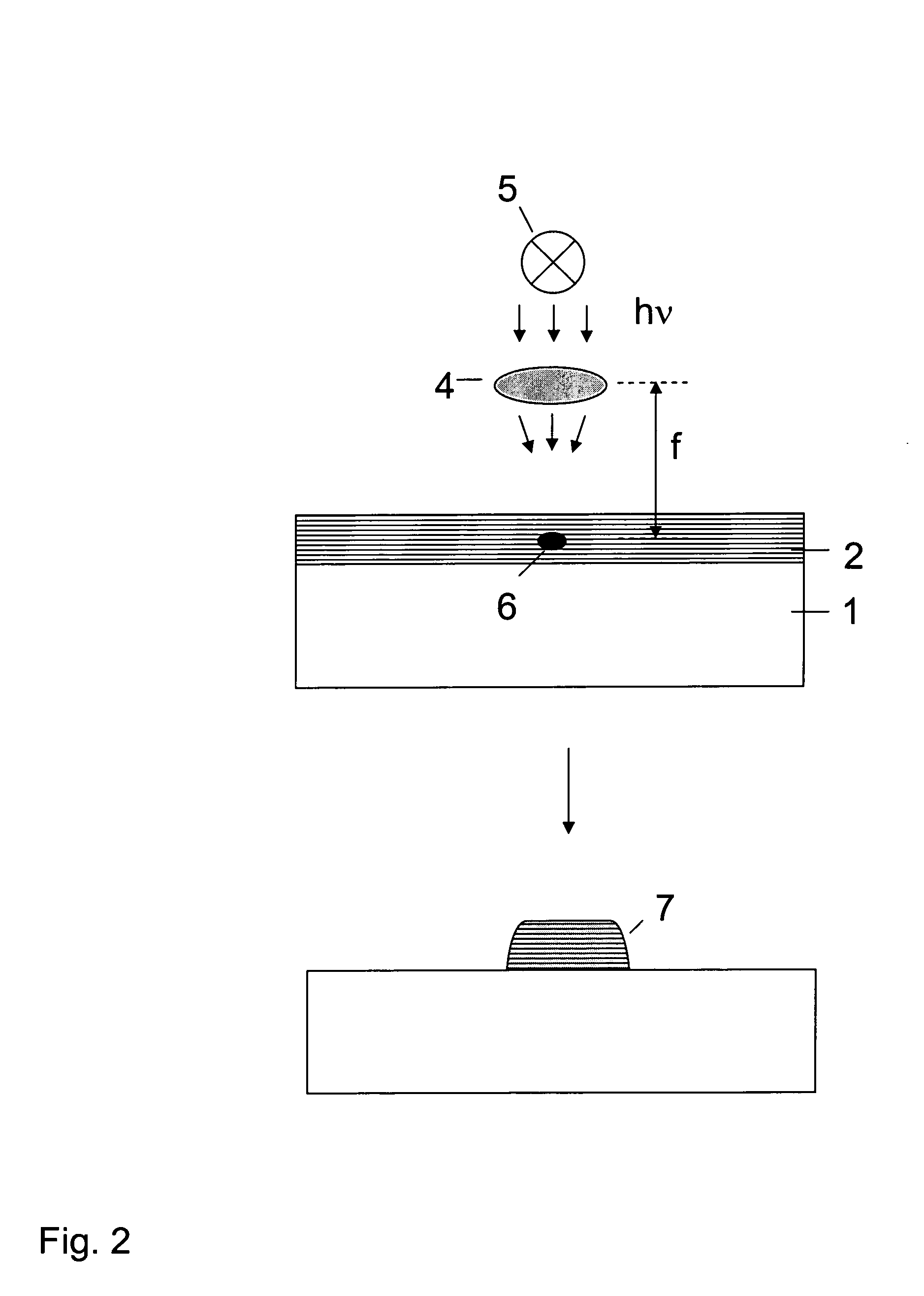
[0037]One embodiment of the present invention relates to a low temperature laser imaging method for direct patterning of an electroactive polymer film 3 that has been coated from solution as a thin continuous film on top of a substrate 1. Suitable deposition techniques to deposit thin films from solution include spin coating, blade coating, extrusion dating or some form of printing, such as screen printing. An intense laser beam (5) of wavelength λ is focussed (4) onto the sample in order to induce a local change in the solubility properties of the electroactive polymer. Preferably, the solubility change is brought about by local heating of the polymer. Preferably, the light beam is of infrared wavelength in order to induce minimum damage to the electroactive polymer. If upon irradiation the polymer becomes insoluble in a particular solvent in which it is soluble in its unirradiated form, a pattern (7) can be produced after local exposure to radiation by washing the polymer film in ...


PUM

PropertyMeasurementUnit
Temperatureaaaaaaaaaa

Abstract

A method for forming an organic or partly organic switching device, comprising: depositing layers of conducting, semiconducting, insulating, or surface modifying layers by solution processing and direct printing; and defining high-resolution patterns of these layers by exposure to a focused laser beam.

Description

[0001]This application is a 371 of PCT / GB02 / 02405 filed May 22, 2002.BACKGROUND OF THE INVENTION[0002]1. Field of the Invention[0003]This invention relates to devices such as organic electronic devices and methods for forming such devices.[0004]2. Description of Related Art[0005]Semiconducting conjugated polymer thin-film transistors (TFTs) have recently become of interest for applications in cheap, logic circuits integrated on plastic substrates (C. Drury, et al., APL 73, 108 (1998)) and optoelectronic integrated devices and pixel transistor switches in high-resolution active-matrix displays (H. Sirringhaus, et al., Science 280, 1741 (1998), A. Dodabalapur, et al. Appl. Phys. Lett. 73, 142 (1998)). In test device configurations with a polymer semiconductor and inorganic metal electrodes and gate dielectric layers high-performance TFTs have been demonstrated. Charge carrier mobilities up to 0.1 cm2 / Vs and ON-OFF current ratios of 106–108 have been reached, which is comparable to the...

Claims


Application Information

Patent Timeline
IPC IPC(8): H01L21/26H01L21/42G03F7/004B41M5/00G03F7/00G03F7/038G03F7/039G03F7/20H01L21/027H01L21/3205H01L21/336H01L21/768H01L29/786H01L51/00H01L51/05H01L51/30H01L51/40
CPCB82Y10/00B82Y40/00G03F7/00H01L21/76894H01L51/0017H01L51/0023H01L51/0016G03F7/0002H01L51/0004H01L51/0541H01L51/0037H01L51/0039H01L51/0516H10K71/13H10K71/221H10K71/231H10K71/621H10K85/1135H10K85/115H10K10/468H10K10/464
Inventor SIRRINGHAUS, HENNINGCAIN, PAUL ALAN
Owner ETV CAPITAL
Why Eureka
Try Eureka