Method of manufacturing light emitting device

a technology of light-emitting devices and manufacturing methods, which is applied in the direction of semiconductor devices, instruments, electrical devices, etc., can solve the problems of cracking in the interface, affecting the generation of holes, and reducing the number of holes injected

Inactive Publication Date: 2007-09-04
SEMICON ENERGY LAB CO LTD
View PDF64 Cites 118 Cited by
  • Summary
  • Abstract
  • Description
  • Claims
  • Application Information

AI Technical Summary

Benefits of technology

[0017]An object of the present invention is therefore to provide a high-quality light emitting device having a long-lasting light emitting element that is free from the problems described above because of a structure that allows less degradation than conventional ones, and to provide a method of manufacturing the light emitting device.

Problems solved by technology

When heat treatment is performed on a structure in which materials having different thermal expansion coefficients are in contact with each other as in this conventional light emitting device structure, it causes a crack in the interface on the side of the material that has the smaller thermal expansion coefficient (the anode, in this case).
If there is a crack in the anode, the crack affects generation of holes, reduces the number of holes injected, and even degrades the light emitting element itself.
The irregularities of the surface of the anode also affect generation and injection of holes.
Furthermore, the organic compound layer is by nature readily degraded by oxygen and moisture.
Moreover, the cathode of the light emitting element is formed of an alkaline metal material, such as Al or Mg, which can seriously impair TFT characteristics.
An alkaline metal mixed in an active layer of a TFT causes a change in electric characteristic of the TFT, making it impossible to give the TFT a long-term reliability.
However, another problem arises when moving a substrate between rooms (clean rooms) is added to the manufacture process in order to prevent the alkaline metal contamination; the TFT substrate may be contaminated by dusts or other contaminants in the air, and the TFT element may be damaged by electrostatic discharge.

Method used


Image

  • Method of manufacturing light emitting device
  • Method of manufacturing light emitting device
  • Method of manufacturing light emitting device

Examples


embodiment 1

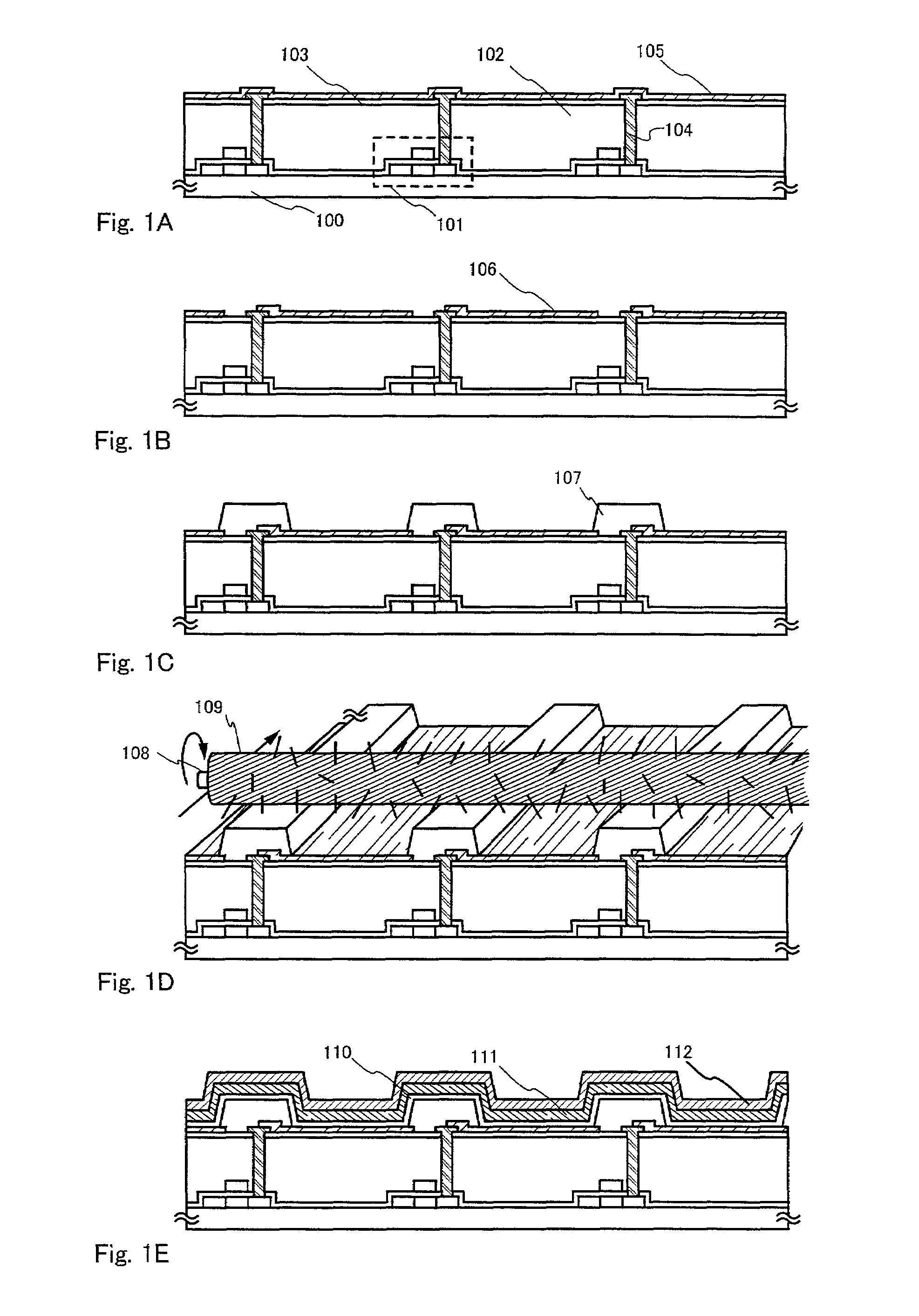
[0065]This embodiment gives a description about a light emitting element that is manufactured using the present invention. Described here with reference to FIGS. 3A to 6B is an example of a method of manufacturing TFTs for a pixel portion and TFTs (an n-channel TFT and a p-channel TFT) for a driving circuit at the same time on the same substrate. The pixel portion has the light emitting element of the present invention. The driving circuit is provided in the periphery of the pixel portion.

[0066]First, a glass substrate 900 is prepared. In this embodiment, barium borosilicate glass, typical example of which is Corning #7059 glass or #1737 glass (product of Coming Incorporated), or alumino borosilicate glass is usable as the substrate 900. The substrate 900 can be any light-transmissive substrate, and a quartz substrate may also be used. A plastic substrate may be employed if it has a heat resistance against the process temperature of this embodiment.

[0067]Next, as shown in FIG. 3A, a...

embodiment 2

[0115]This embodiment describes another example of process of manufacturing a light emitting device with reference to FIGS. 19 to 22B.

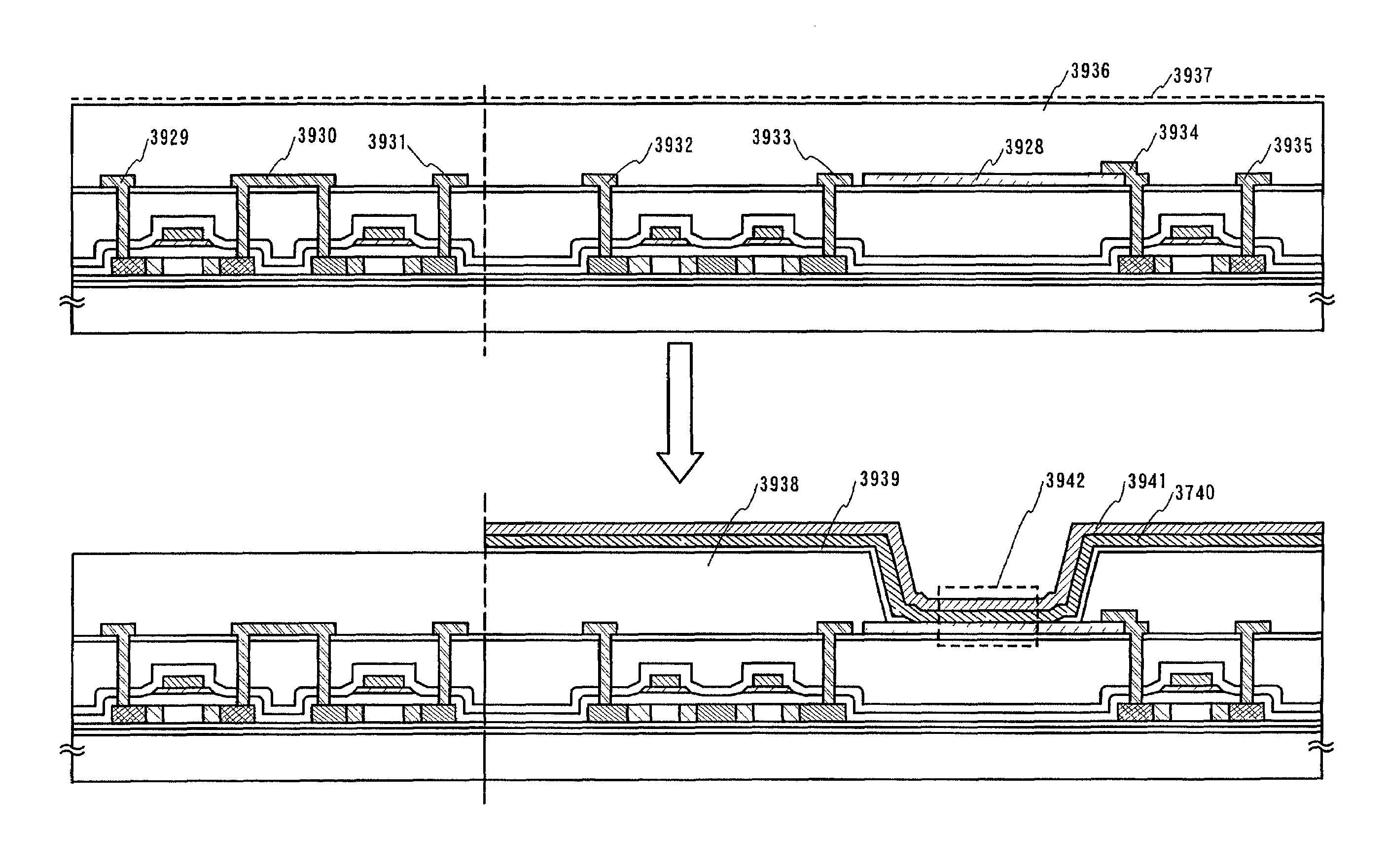
[0116]Following the description in Embodiment 1, the steps up through the step of forming two layers of conductive films 907 and 908 on the gate insulating film 906 as shown in FIG. 3A are finished.

[0117]Subsequently, a process where the conductive films 907 and 908 are etched using masks 909a to 909d to form conductive layers 3901 to 3904 having a first taper shape is described in FIG. 20A. ICP (inductively coupled plasma) etching is used for this etching. Though etching gas is not limited, CF4, Cl2, and O2 are used to etch a W film and a tantalum nitride film. The gas flow rate of CF4, Cl2, and O2 is respectively set to 25 / 25 / 10, and RF (13.56 MHz) power of 500 W is given to a coiled electrode at a pressure of 1 Pa for the etching. RF (13.56 MHz) power of 150 W is also given to the substrate side (sample stage) so that substantially negative self-bi...

embodiment 3

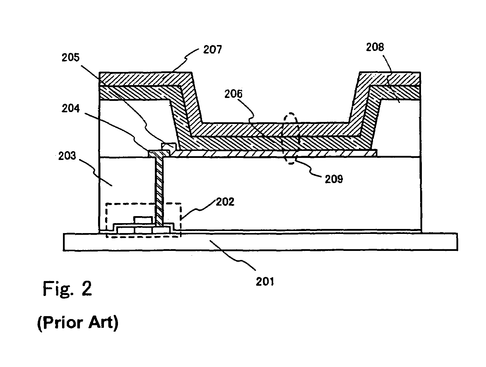
[0139]Following the description of Embodiment 1 or 2, the manufacture process up through the step of forming the second interlayer insulating film (935 or 3926) is finished. Then, instead of forming the first insulating film 936 of Embodiment 1, plasma treatment is performed on the second interlayer insulating film to modify the surface of the second interlayer insulating film (935 or 3926). This method will be described with reference to FIG. 7.

[0140]The second interlayer insulating film (935 or 3926) receives plasma treatment in, for example, one or more kinds of gas selected from the group consisting of hydrogen, nitrogen, hydrocarbon, halogenated carbon, hydrogen fluoride, and rare gas (such as Ar, He, or Ne), so that a coat is newly formed on the surface of the second interlayer insulating film (935 or 3926) or the existing functional group on the surface is changed to a different functional group. The surface modification of the second interlayer insulating film (935 or 3926) ...


PUM


Abstract

A high-quality light emitting device is provided which has a long-lasting light emitting element free from the problems of conventional ones because of a structure that allows less degradation, and a method of manufacturing the light emitting device is provided. After a bank is formed, an exposed anode surface is wiped using a PVA (polyvinyl alcohol)-based porous substance or the like to level the surface and remove dusts from the surface. An insulating film is formed between an interlayer insulating film on a TFT and the anode. Alternatively, plasma treatment is performed on the surface of the interlayer insulating film on the TFT for surface modification.

Description

BACKGROUND OF THE INVENTION[0001]1. Field of the Invention[0002]The present invention relates to a light emitting device with a light emitting element composed of an anode, a cathode, and a film that contains an organic compound capable of emitting light upon application of electric field (the film is hereinafter referred to as organic compound layer), and to a method of manufacturing the light emitting device. Specifically, the present invention relates to a light emitting device using a light emitting element that is lower in drive voltage and longer in element lifetime than conventional ones. A light emitting device in this specification refers to an image display device that uses a light emitting element. Also, the following modules are all included in the definition of the light emitting device: a module obtained by attaching to a light emitting element a connector such as an anisotropic conductive film (FPC: flexible printed circuit), a TAB (tape automated bonding) tape, or a ...

Claims


Application Information

Patent Timeline
Patent Type & Authority Patents(United States)
IPC IPC(8): H01L21/56G09G3/30H01L27/32
CPCH01L27/3246H01L27/3258H01L51/5206H01L51/524H01L51/56Y10S438/976H01L51/5253H10K59/122H10K59/124H10K50/81H10K50/844G09G3/30H10K50/841H10K50/805H10K71/00H10K50/15H10K71/12
Inventor YAMAGATA, HIROKAZUYAMAZAKI, SHUNPEITAKAYAMA, TORU
Owner SEMICON ENERGY LAB CO LTD
Why Eureka
Try Eureka