

Organic underlayers that improve the performance of organic semiconductors
a technology of organic semiconductors and underlayers, which is applied in the direction of semiconductor devices, material nanotechnology, electrical equipment, etc., can solve the problems of surface roughness and adversely affect the size of pentacene crystals, and achieve the effect of high performance and maximize the mobility of charge carriers
- Summary
- Abstract
- Description
- Claims
- Application Information
AI Technical Summary
Benefits of technology
Problems solved by technology
Method used
Image

Examples
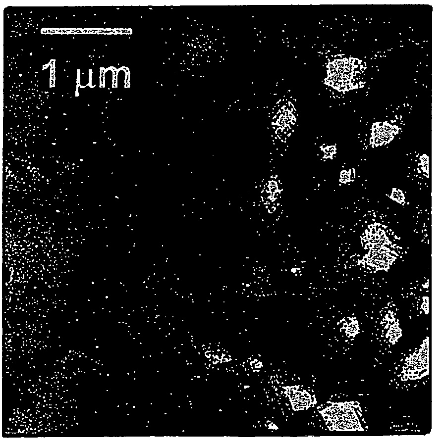
example 1
[0064]Highly doped silicon wafers with 5000 Å of thermally grown oxide were cleaned using chloroform, UV / ozone, and a heated solution of sulfuric acid and hydrogen peroxide, followed by rinsing and drying. The samples were immersed in 1 millimolar solutions of the following silanes in anhydrous hexane: octadecyltrichlorosilane, phenyltrichlorosilane, cyclopentyltrichlorosilane, cyclotetramethylenedichlorosilane, and 1,1-diethoxy-1-silacyclopent-3-ene, as well as an untreated wafer that was used as a control. The solutions were heated to 50° C., and the samples remained in contact with the silane solution overnight. The samples were rinsed several times in fresh hexane and dried in an inert atmosphere. The samples were baked at 50° C. for 10 minutes to promote the reaction of any unreacted chlorosilane groups. An approximately 300 Å thick film of pentacene was deposited onto the samples through a metal shadow mask using molecular beam deposition techniques. Source and drain electrode...
example 2
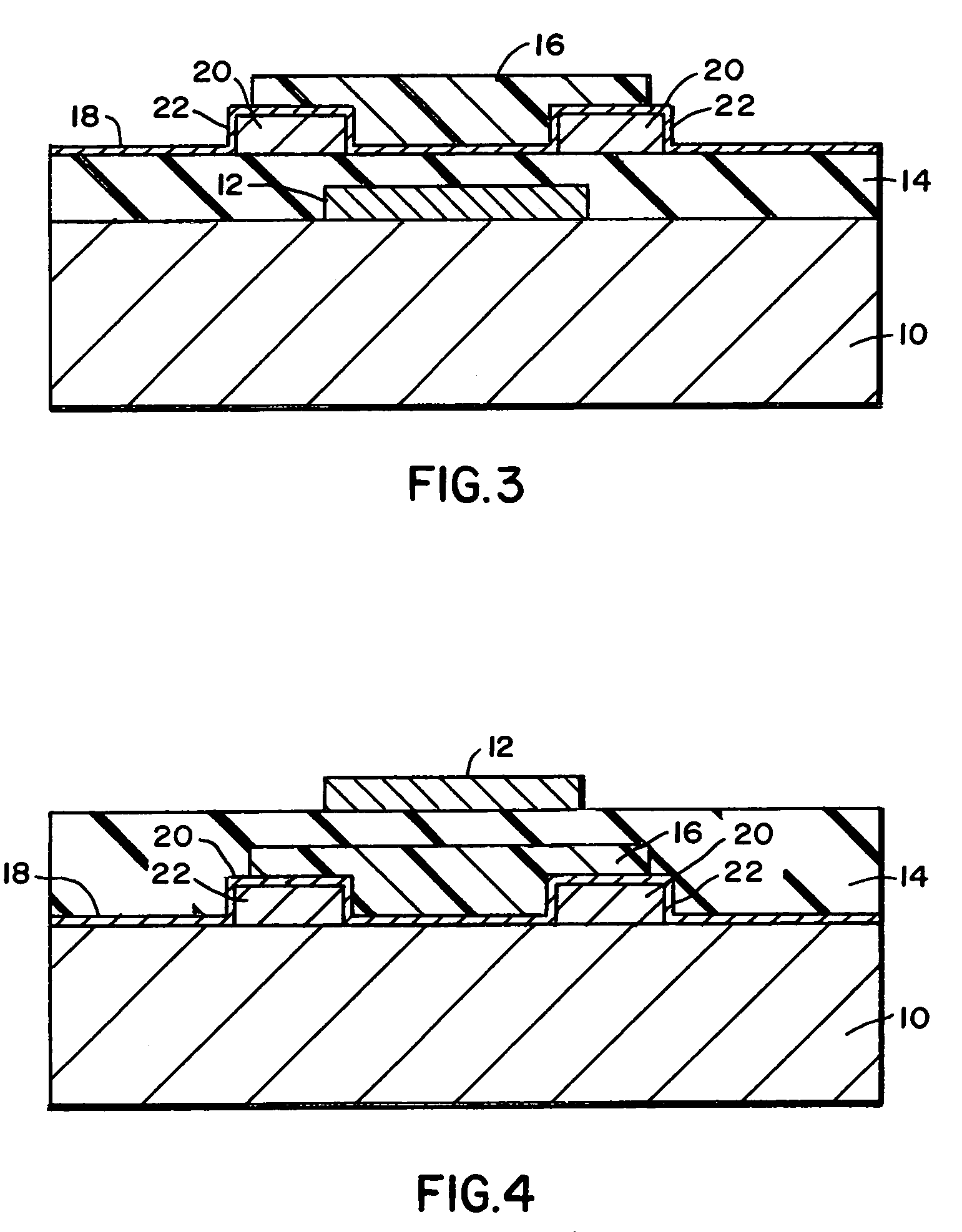
[0068]Bottom contact devices, as depicted in the cross section in FIG. 3, require monolayers to be applied on both the gate insulator and the electrodes to produce a uniform surface for pentacene deposition. In these cases, highly doped silicon wafers with 5000 Å of thermally grown oxide were cleaned using chloroform, UV / ozone, and a heated solution of sulfuric acid and hydrogen peroxide, followed by rinsing and drying. Patterned gold or gold on chromium contacts were deposited by evaporation through a metal shadow mask. Samples were immersed in 1 millimolar solutions of octadecyltrichlorosilane or 1,1-diethoxy-1-silacyclopent-3-ene in anhydrous hexane, and untreated samples were used as controls. The solutions were heated to 50° C., and the samples remained in contact with the silane solution overnight. The samples were rinsed several times in fresh hexane and dried in an inert atmosphere. The samples were baked at 50° C. for 10 minutes to promote the reaction of any unreacted chlo...
PUM
| Property | Measurement | Unit |
|---|---|---|
| temperature | aaaaa | aaaaa |
| thickness | aaaaa | aaaaa |
| thickness | aaaaa | aaaaa |
Abstract
Description
Claims
Application Information