Nanoscale programmable structures and methods of forming and using same

a programmable structure and nano-scale technology, applied in the field of programmable structures, can solve the problems of undesirable forming of memory devices and other devices on separate substrates, requiring a relatively large amount of space within the system, and forming various types of memory on separate substrates may be relatively expensive, so as to achieve the effect of reducing the drift of the devi

Inactive Publication Date: 2007-11-13
AXON TECH
View PDF5 Cites 49 Cited by
  • Summary
  • Abstract
  • Description
  • Claims
  • Application Information

AI Technical Summary

Benefits of technology

[0008]While the ways in which the present invention addresses the various drawbacks of typical programmable memory devices will be discussed in greater detail below, in general, the devices and structures of the present invention are relatively easy to manufacture, are relatively inexpensive, consume relatively small amounts of power, and can be scaled down to relatively small sizes.
[0013]In accordance with yet another embodiment of the invention, a structure is programmed using a sufficient voltage and current to mitigate any drift in the device.

Problems solved by technology

Forming memory devices and other devices on separate substrates may be undesirable for several reasons.
For example, forming various types of memory on separate substrate may be relatively expensive, may require relatively long transmission paths to communicate between the memory devices and any associated electronic device, and may require a relatively large amount of room within a system.
Furthermore, as the semiconductor and microelectronics industries continue down the roadmap of ever decreasing the size of memory devices, several problems with existing memory technologies arise.
For example, as the physical size of charge-storage devices such as FLASH and DRAM devices decreases, state detection and / or retention of the devices deteriorate.
With other typical semiconductor memory devices, power consumption and cost of the devices generally increase as the size of the devices decreases.

Method used


Image

  • Nanoscale programmable structures and methods of forming and using same
  • Nanoscale programmable structures and methods of forming and using same
  • Nanoscale programmable structures and methods of forming and using same

Examples


example i

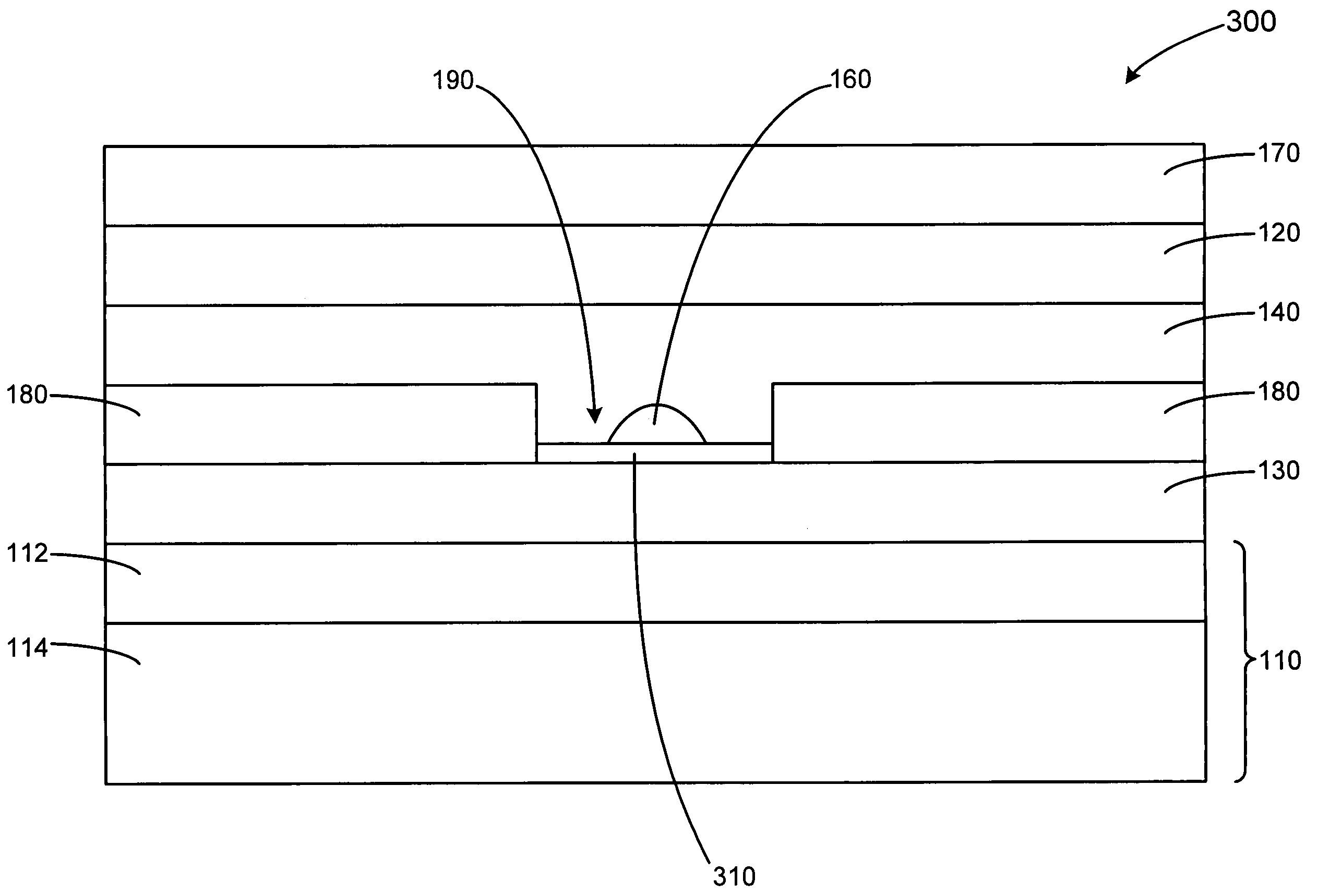
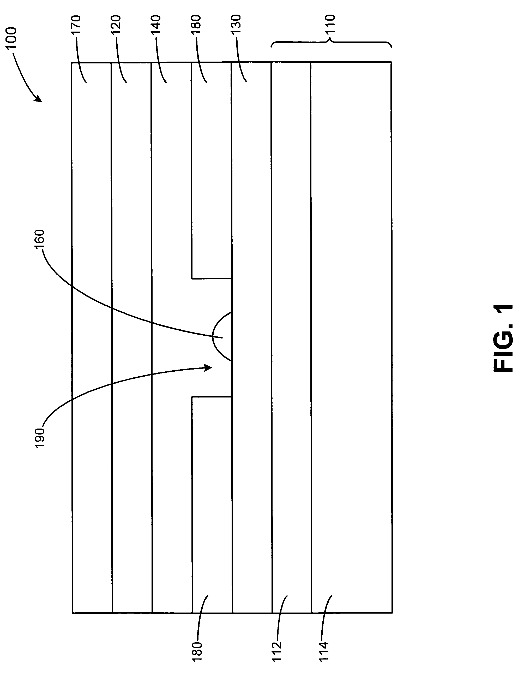
[0046]A 100 nm thick silicon oxide layer is grown on a silicon substrate. Next, a first electrode material (e.g., 100-200 nm of Ni) is deposited onto the silicon oxide. The first electrode material is patterned (e.g., using optical lithography) to form the bottom inert electrodes. Immediately following first electrode material patterning (to avoid significant ambient surface contamination of the material), electron-beam resist (e.g., 100 nm of PMMA) is deposited over the silicon oxide and first electrode material. The resist is applied by spin casting and the resist is baked at 170° C. for about 18 hours to ensure complete solvent removal. The insulting material is then patterned by exposing the PMMA using a JEOL 6000 e-beam lithography system having an area dose of 1200 μC / cm2 to define nanoscale openings aligned to the bottom electrode. The resist is then developed by exposing the patterned resist for 20 seconds in a developer including 11:10:1 MIBK:CS:MEK (MIBK is 1:3 methyl isob...

example ii

[0052]This process is the same as the process of Example I, with the exception of the electron beam parameters, the Ag dissolution is performed using UV light only, and a gold top electrode is added to prevent tarnishing of the silver.

[0053]Following the deposition of the PMMA, the PMMA is exposed at 800 μC / cm2 using the JEOL 6000 EBL system and the patterns are developed described above. Approximately 50 nm of Ge30Se70 in then evaporated at 0.05 nm / sec along with a 30 nm thick Ag overlayer and the Ag is diffused by exposing the metal to 405 nm UV radiation at an energy of 1 J / cm2 to ensure Ag penetration throughout the entire thickness of the electrolyte film. A top electrode bilayer of 80 nm of Ag and 50 nm of Au is then deposited. This stack is then patterned using optical lithography and a combination of sputter etching (to pattern the Au) and wet etching as described above.

[0054]Methods of Programming and Using the Device and Structure

[0055]As noted above, information may be st...


PUM


Abstract

A programmable structure and device and methods of forming and using the structure and device are disclosed. The structure includes a soluble electrode, an ion conductor, and an inert electrode. Upon application of a sufficient voltage, a conductive region forms within or on the ion conductor and between the electrodes. The presence or absence of the conductive region can be used to store information in memory devices.

Description

CROSS REFERENCE TO RELATED APPLICATIONS[0001]This application is a continuation-in-part of and claims priority to, and the benefit of, U.S. patent application Ser. No. 10 / 458,551 entitled SCALABLE PROGRAMMABLE STRUCTURE, AN ARRAY INCLUDING THE STRUCTURE, AND METHODS OF FORMING THE SAME, filed Jun. 9, 2003, which claims the benefit of U.S. Provisional Application Ser. No. 60 / 387,204, entitled PROGRAMMABLE METALLIZATION CELL WITH INTEGRAL SERIES DIODE, filed Jun. 7, 2002 and U.S. Provisional Application Ser. No. 60 / 390,793, entitled MICROELECTRONIC DEVICE, STRUCTURE, AND SYSTEM, INCLUDING A MEMORY STRUCTURE HAVING A VARIABLE PROGRAMMABLE PROPERTY AND METHOD OF FORMING THE SAME, filed Jun. 19, 2002. This application also claims priority to Provisional Application Ser. No. 60 / 579,540, entitled NANOSCALE MEMORY ELEMENTS BASED ON SOLID-STATE ELECTROLYTES, filed Jun. 14, 2004. All four applications are hereby incorporated by reference in their entirety.FIELD OF INVENTION[0002]The present i...

Claims


Application Information

Patent Timeline
Patent Type & Authority Patents(United States)
IPC IPC(8): H01L27/148G11C13/02G11C16/02H01L29/06H01L45/00
CPCG11C13/0007H01L45/085H01L45/1233H01L45/142H01L45/143H01L45/144H01L45/146H01L45/1675H01L45/1683G11C13/0011Y10S977/943G11C2213/15G11C2213/32G11C2213/34G11C2213/51Y10S977/81Y10S977/831H10N70/245H10N70/826H10N70/8822H10N70/8825H10N70/8828H10N70/8833H10N70/063H10N70/066
Inventor KOZICKI, MICHAEL N.
Owner AXON TECH
Why Eureka
Try Eureka