Semiconductor laser module and method of assembling the same

a laser module and semiconductor technology, applied in semiconductor lasers, optical elements, instruments, etc., can solve the problems of not being able to integrate the semiconductor laser element and the semiconductor optical amplifier in one chip with the existing semiconductor manufacturing technology, and achieve the effect of reducing the size of the optical transmission module and high yield

Inactive Publication Date: 2007-12-11
NEC CORP
View PDF25 Cites 12 Cited by
  • Summary
  • Abstract
  • Description
  • Claims
  • Application Information

AI Technical Summary

Benefits of technology

[0034]An object of the present invention is to provide a semiconductor laser module and a method of assembling the same which ...

Problems solved by technology

In this case, it is impossible to install the semiconductor laser element and the semico...

Method used


Image

  • Semiconductor laser module and method of assembling the same
  • Semiconductor laser module and method of assembling the same
  • Semiconductor laser module and method of assembling the same

Examples


first embodiment

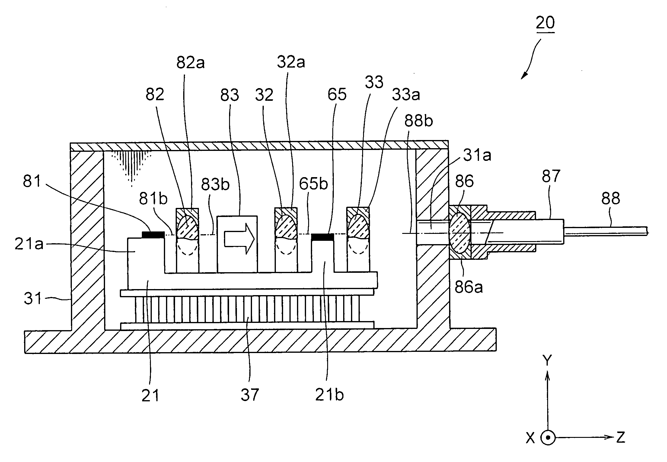
[0061]Next, with reference to FIG. 6, the present invention will be described by referring to a case where: a semiconductor laser element (in the followings, referred to as a DFB laser element) 81 as a first semiconductor optical element for outputting laser light; and a semiconductor optical amplifier (in the followings, referred to as an SOA element) 65 as the second semiconductor optical element, which amplifies the light signal by exciting it in an active layer through supplying an electric current and outputs the amplified light signal, are used. The semiconductor optical elements are not limited to the semiconductor laser element and the semiconductor amplifier but other elements may be used.

[0062]As shown in FIG. 6, an element carrier 21 is enclosed inside a package 31 by being supported by a Peltier element 37 as an electronic cooling element. The element carrier 21 comprises, on one face (surface), an element holding section 21a to which the DFB laser element 81 is mounted ...

second embodiment

[0090]FIG. 9 is a block diagram showing the laser module according to the present invention. FIG. 10 is a front elevational view of the optical element holder shown in FIG. 9 viewed from the Z direction. In the followings, description will be provided by referring to the drawings. In FIG. 9 and FIG. 10, the same numeral codes are applied to the identical parts as the ones used in FIG. 6 to FIG. 8, and the description will be omitted.

[0091]Basically, a laser module 30 of the embodiment comprises: a DFB laser element 81 for outputting signal light; an SOA element 65 for amplifying the signal light outputted from the DFB laser element 81; an element carrier 16 to which the DFB laser element 81 and the SOA element 65 are fixed with the optical axes being adjusted with each other; an optical element holder 10 for fixing the SOA element 65 to the element carrier 16; a package 31 for enclosing the DFB laser element 81, the SOA element 65, the element carrier 16 and the optical element hold...


PUM


Abstract

Provided are a semiconductor laser module and a method of assembling the same. The semiconductor laser module comprises a first semiconductor optical element and a second semiconductor optical element as a pair and a lens. The first semiconductor optical element is for outputting light signal and the second semiconductor optical element is for performing signal processing on the light signal outputted from the first semiconductor optical element. The lens is for correcting a relation between optical axes of the first semiconductor optical element and the second semiconductor optical element so as to lens-couple the optical axes. The first semiconductor optical element, the second semiconductor optical element and the lens are mounted on a common element carrier.

Description

BACKGROUND OF THE INVENTION[0001]1. Field of the Invention[0002]The present invention relates to a semiconductor laser module used in the field of optical communication technology and a method of assembling the same.[0003]2. Description of the Related Art[0004]The optical communication system has grown with merits of having a large capacity and achieving a long distance transmission. As for the improved capacity of the optical communication system, information transmission of up to 10 Gbits has been made into practical use by improving the speed for modulating the light signal.[0005]As for the increased transmission distance of the optical communication system, the transmission distance which can be achieved without a relay exceeds 100 km by combining an optical fiber in which losses of the optical transmission is small with an erbium-doped optical fiber amplifier (in the followings, referred to as EDFA).[0006]However, the EDFA is formed with a large number of optical components suc...

Claims


Application Information

Patent Timeline
IPC IPC(8): H01S3/04H01S5/00G02B6/42H01S5/022
CPCH01S5/02284G02B6/4237H01S5/005H01S5/0064H01S5/02216H01S5/02438H01S5/02288H01S5/02415H01S5/02252H01S5/02251H01S5/02253H01S5/02326
Inventor NAMIWAKA, MASAHIKOKANEKO, TARO
Owner NEC CORP
Why Eureka
Try Eureka