Structure having pores, device using the same, and manufacturing methods therefor

a technology of pores and pores, applied in the direction of filtration separation, separation processes, instruments, etc., can solve the problems of low production yield, limited application and shape, and high cost of apparatuses therefor, and achieve the effect of a new and effective minute structur

Inactive Publication Date: 2008-01-15
CANON KK
View PDF16 Cites 30 Cited by
  • Summary
  • Abstract
  • Description
  • Claims
  • Application Information

AI Technical Summary

Benefits of technology

[0013]Accordingly, it is an object of the present invention to solve the problems described above and to provide a novel and effective minute structure.
[0015]Another aspect of the present invention is to provide a minute structure in which a material is selectively filled in some of the plurality of pores disposed above a substrate and to provide a manufacturing method therefor.

Problems solved by technology

Concerning the formation of a nanostructure by using semiconductor processing techniques described above, there are problems in that the production yield is low and the apparatuses therefor are costly.
Since the nanostructure shown in FIG. 9 is only formed on an Al plate surface, the application and the shape thereof are limited to some extent.

Method used


Image

  • Structure having pores, device using the same, and manufacturing methods therefor
  • Structure having pores, device using the same, and manufacturing methods therefor
  • Structure having pores, device using the same, and manufacturing methods therefor

Examples


example 1

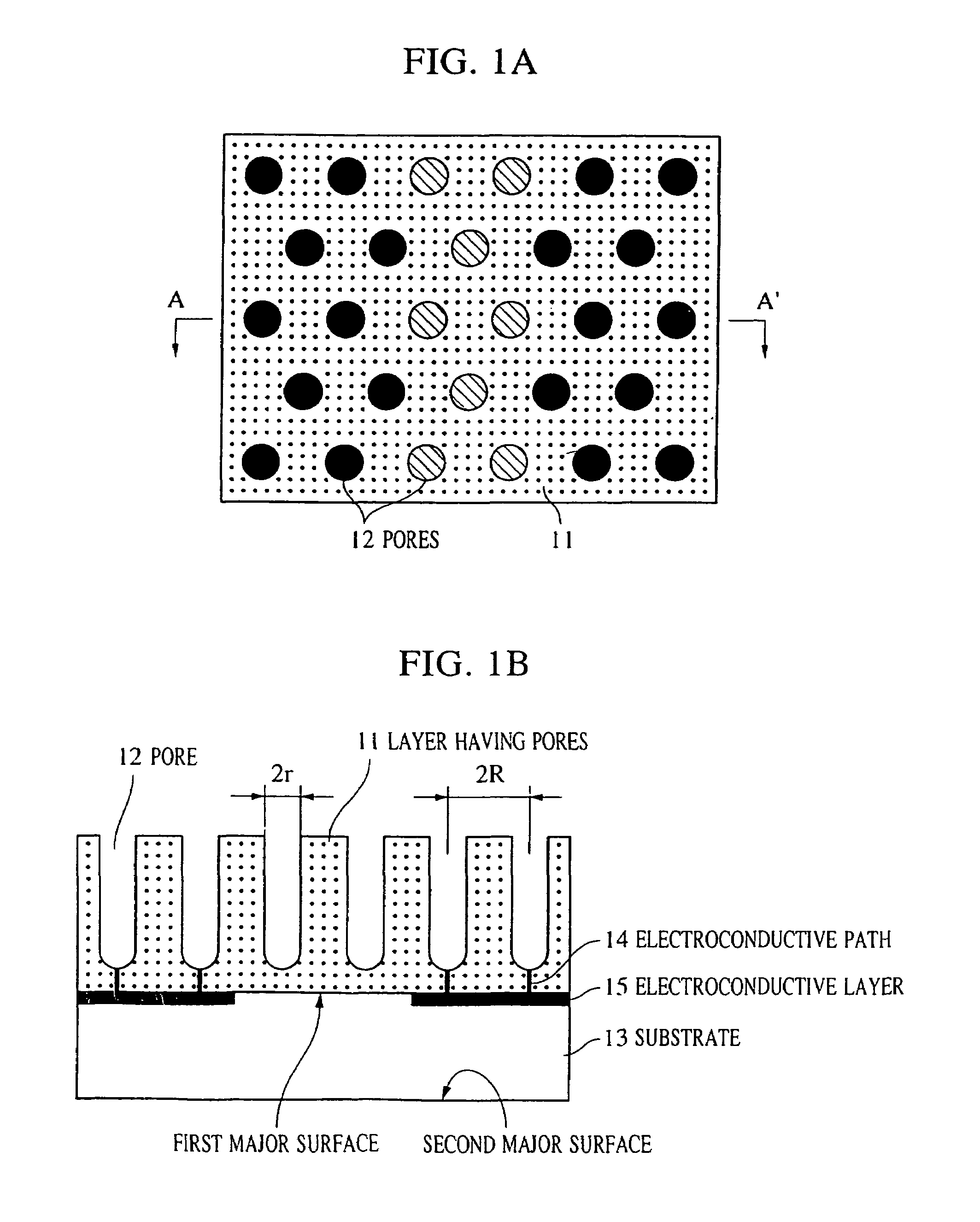
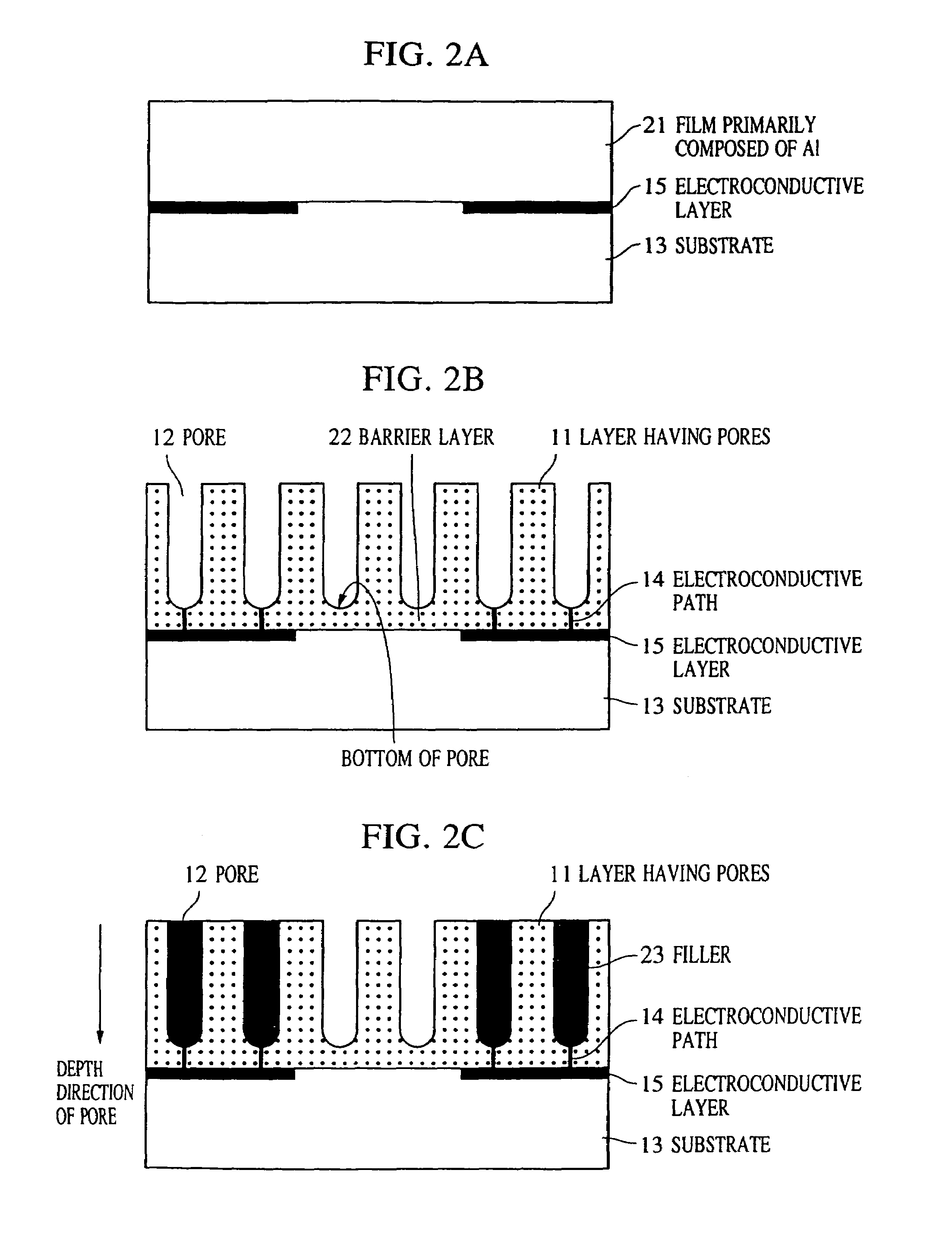
[0104]In this example, electrodeposition and the shapes of pores when aluminum nanohole layers are formed using various electroconductive layers will be described with reference to FIGS. 2A to 2C. Seven samples were made. In each sample, materials used to make the electroconductive films 15 are different from each other.

a) Formation of Electroconductive Layer 15 and Al Film 21

[0105]A resist (Hitachi Chemical Co., Ltd., RD-2000N) 1 μm thick was formed by spin-coating on a quartz substrate 13, and a line 10 μm wide was then exposed using a mask and developed. Subsequently, an electroconductive film 100 nm thick was formed by RF sputtering. As a material for the electroconductive films, Ti, Zr, Hf, Nb, Ta, Mo, and W were respectively used to each sample. The conditions for film formation were set so that the pressure in an Ar atmosphere was 30 mTorr, and the RF power was 500 W. By peeling the resist using a lift-off method, a 10 μm-wide electroconductive layer 15 was formed.

[0106]Subse...

example 2

[0118]In this example, an anodized alumina nanohole layer was formed in a manner similar to that in Example 1.

[0119]In this example, a substrate 13 was a quartz substrate, and W was sputtered on the substrate 13 so as to be 100 nm thick and was then patterned by a lift-off method. Anodization was performed in a solution of oxalic acid at a voltage of 40 V at a bath temperature of 10° C. and was completed 10 minutes after passing the point C in FIG. 4 at which the anodizing current was sufficiently low. Similarly to Example 1, a pore-widening treatment was performed in a solution of 5 percent by weight of phosphoric acid for 40 minutes.

[0120]The sample and a counter electrode made of platinum were immersed in an electrolyte composed of cobalt sulfate at a concentration of 0.5 M and copper sulfate at a concentration of 0.005 M, and an alternating voltage of 5 V at 50 Hz was applied between the sample and the counter electrode, whereby nuclei of an alloy composed of cobalt and copper w...

example 3

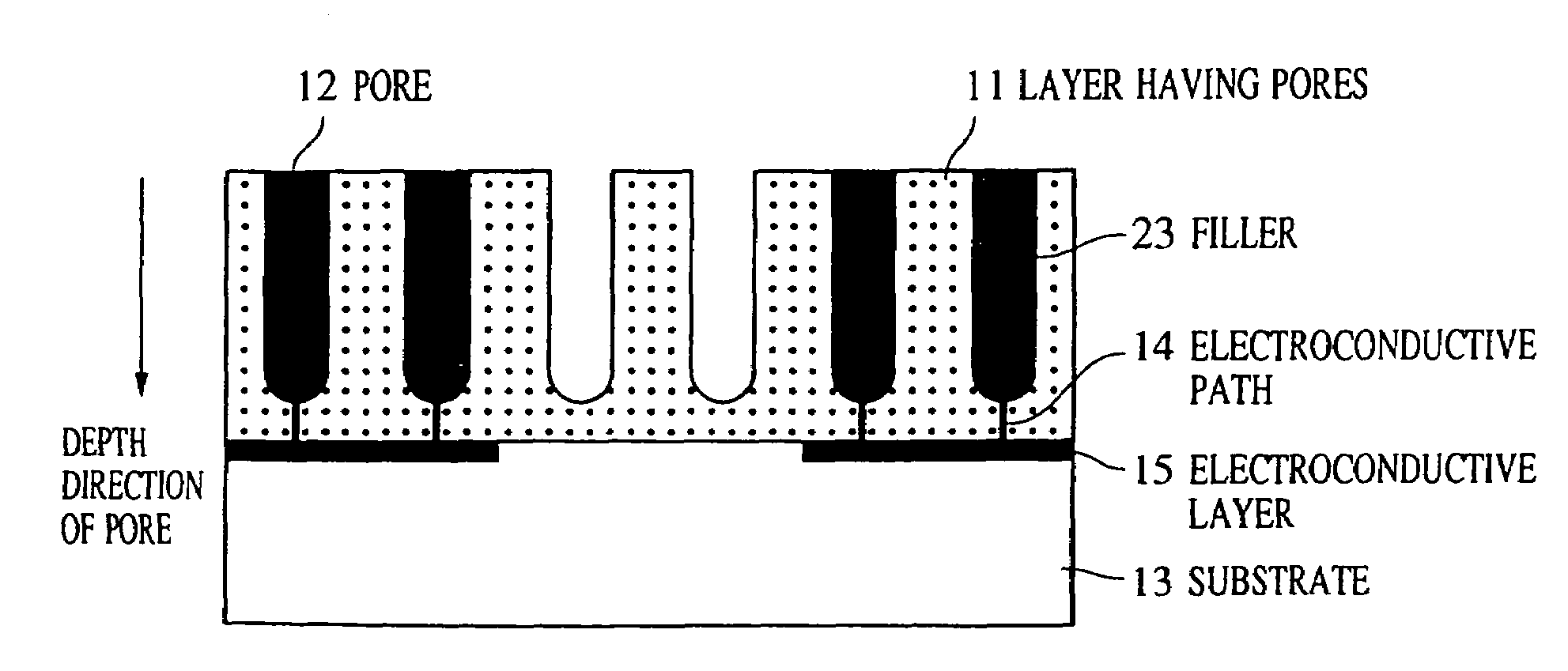
[0124]In this example, formation of an alumina nanohole layer provided with a patterned electroconductive layer 15 composed of Nb formed on a quartz substrate 13 and infiltration of an oxide in pores 12 were performed.

[0125]On the quartz substrate 13 provided with the 100 nm-thick patterned electroconductive layer 15 composed of Nb, a 5 μm-thick Al film 21 was formed (FIG. 2A).

[0126]Next, recesses arranged in the form of a honeycomb (a hexagonal grating) were formed on the surface of the Al film 21 by lithography. The space between recesses was set to be 300 nm.

[0127]Subsequently, by performing anodization in a manner similar to that in Example 1, pores 12 (nanoholes) were formed above the substrate 13. In the anodization, a solution of phosphoric acid at a concentration of 0.3 M was used as an electrolyte, the voltage was set to be 140 V, and the completion of anodization was set to be at a time sufficiently long after a decrease in current at the point C in FIG. 4. A pore-widening...


PUM

PropertyMeasurementUnit
aspect ratiosaaaaaaaaaa
melting pointaaaaaaaaaa
thicknessaaaaaaaaaa

Abstract

A minute structure is provided in which electroconductive paths are only formed in nanoholes, and a material is filled in the nanoholes, which are disposed in a specific area, by using the electroconductive paths. The minute structure comprising pores comprises a) a substrate, b) a plurality of electroconductive layers formed on a surface of the substrate, c) a layer primarily composed of aluminum oxide covering the plurality of electroconductive layers and a surface of the substrate where no electroconductive layer is formed, and d) a plurality of pores formed in the layer primarily composed of aluminum oxide, in which the pores are disposed above the electroconductive layers and the surface of the substrate where no electroconductive layers is formed, with a part of the layer primarily composed of aluminum oxide provided under the bottoms of the pores, and in which the layer primarily composed of aluminum oxide provided between the electroconductive layer and the bottoms of the pores disposed above the electroconductive layer comprises a material forming the electroconductive layer.

Description

[0001]This application is a divisional of application Ser. No. 09 / 666,605, filed Sep. 20, 2000 now abandoned, the contents of which are incorporated herein by reference.BACKGROUND OF THE INVENTION[0002]1. Field of the Invention[0003]The present invention relates to minute structures, devices having minute structures, and manufacturing methods thereof. In particular, the present invention relates to a nanoscale structure, a device using the nanoscale structure, and manufacturing methods thereof. The nanoscale structure of the present invention provided with alumina nanoholes can be widely used as a functional material and as a structural material for electronic devices and micro devices. The present invention can be particularly applied to quantum effect devices, electrochemical sensors, biosensors, magnetic memory devices, magnetic devices, light-emitting devices, photonic devices, solar cells, and the like.[0004]2. Description of the Related Art[0005]Since the movement of electrons...

Claims


Application Information

Patent Timeline
Patent Type & Authority Patents(United States)
IPC IPC(8): H01L21/44B82B1/00B81B1/00H01J1/304H01L43/08H01L43/12H01L49/02
CPCB81B1/002B81C1/00031B81B2201/0214H01L43/12Y10S977/781Y10S977/893H10N50/01
Inventor DEN, TOHRUIWASAKI, TATSUYA
Owner CANON KK
Why Eureka
Try Eureka