

Organoelement resists for EUV lithography and methods of making the same
a technology of organic elements and resists, applied in the field of organic element resists, can solve the problems of affecting the etching process, the inability to resist the current etching technique, and the strain on the existing lithography technology, so as to improve the method of forming features on the substra
- Summary
- Abstract
- Description
- Claims
- Application Information
AI Technical Summary
Benefits of technology
Problems solved by technology
Method used
Image

Examples
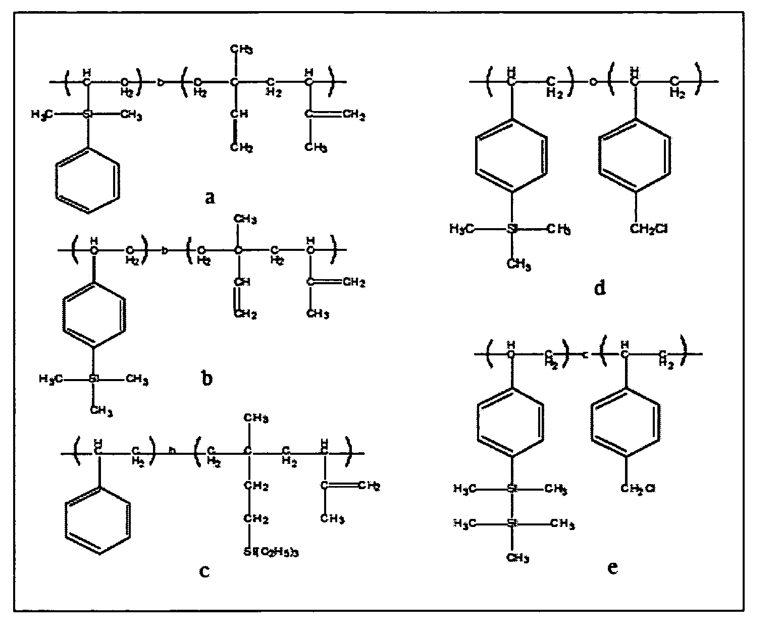
example 1
Formation of poly(dimethylphenylvinylsilane-b-isoprene)
[0076]Dimethylphenylvinylsilane and isoprene were distilled from CaH2 and dibutylmagnesium successively under high vacuum prior to use. Toluene was dried by distillation from CaH2 and degassed three times prior to its use as a solvent. The poly(dimethyl-phenylvinylsilane-b-isoprene) was synthesized by living anionic polymerization using standard high vacuum techniques. The polymerization was initiated by s-Butyl lithium and was quenched with anhydrous methanol.
example 2
Formation of poly(trimethylsilylstyrene-b-isoprene)
[0077]Trimethylsilylstyrene was synthesized and then distilled successfully from CaH2 and dibutylmagnesium under a high vacuum. Poly(trimethylsilylstyrene-b-isoprene) was synthesized by living anionic polymerization of the distilled trimethylsilylstyrene with isoprene in tetrahydrofuran using standard high vacuum techniques.
example 3
Formation of poly(trimethysilylstyrene-co-chloromethylstyrene)
[0078]Numerous samples of poly(trimethylsilylstyrene-co-chloromethylstyrene) having different compositions were synthesized by the free radical polymerization of trimethylsilylstyrene and chloromethylstyrene in tetrahydrofuran using azobisisobutyronitrile (AIBN) as an initiator. The polymerizations were performed at 65° C. The polymer solution was precipitated in methanol, re-dissolved in tetrahydrofuran, and then re-precipitated in methanol. The samples were dried in vacuo overnight.
PUM
| Property | Measurement | Unit |
|---|---|---|
| Percent by mass | aaaaa | aaaaa |
| Structure | aaaaa | aaaaa |
| Electrical resistance | aaaaa | aaaaa |
Abstract
Description
Claims
Application Information