Photomask blank, photomask, and method of manufacture

a technology of photomask and blank, applied in the field of photomask blank, photomask and method of manufacture, can solve the problems of restricting compositional and limiting the freedom of design in positively improving, and achieve good perpendicularity in etched cross-sectional geometry, and precise patterning

Active Publication Date: 2008-02-12
SHIN ETSU CHEM CO LTD
View PDF21 Cites 2 Cited by
  • Summary
  • Abstract
  • Description
  • Claims
  • Application Information

AI Technical Summary

Benefits of technology

[0016]An object of the invention is to provide a photomask blank, typically a phase shift mask blank, which affords a photomask that satisfies optical properties such as transmittance, reflectance and refractive index at an exposure wavelength of interest, and has an etched pattern with a minimal line edge roughness, that is, a photomask having an improved etched cross-sectional geometry upon mask pattern formation; a photomask, typically a phase shift mask obtained therefrom; and methods of manufacturing the photomask blank and the photomask. A further object is to provide a phase shift mask blank which exhibits good perpendicularity in etched cross-sectional geometry upon mask pattern formation by reactive ion etching (RIE); a phase shift mask obtained therefrom; and methods of manufacturing the phase shift mask blank and the phase shift mask.

Problems solved by technology

However, a restrictive compositional range of zirconium silicide compound coating and molybdenum silicide compound coating is required to eliminates steps in etched cross-section.
This limits the freedom of design in positively improving the cross-sectional geometry of an etched pattern (the inclination angle of sidewall).

Method used


Image

  • Photomask blank, photomask, and method of manufacture
  • Photomask blank, photomask, and method of manufacture
  • Photomask blank, photomask, and method of manufacture

Examples


example

[0148]Examples and comparative examples are given below by way of illustration, and are not intended to limit the scope of the invention.

first embodiment

Example 1

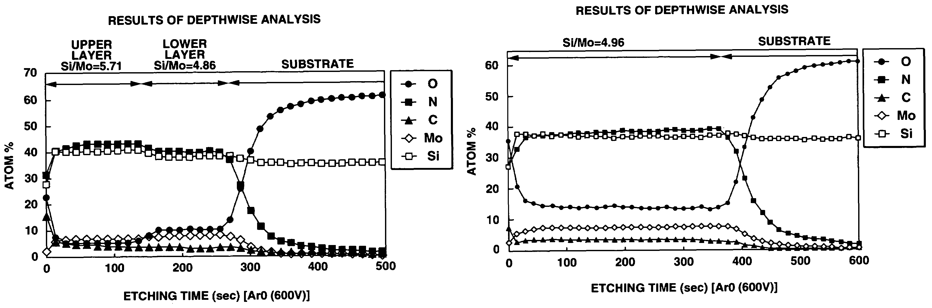
[0149]A multilayer film (phase shift multilayer film) was prepared by depositing alternate layers of molybdenum silicide oxynitride (MoSiON) and silicon oxynitride (SiON).

[0150]For the deposition, a dc sputtering system including two targets 33a and 33b as shown in FIG. 11 was used. The target 33a for MoSiON layers was a MoSi3.5 target and the target 33b for SiON layers was a Si target. The sputtering gas was a gas mixture of 20 cm3 / min of Ar, 100 cm3 / min of N2 and 5 cm3 / min of O2. A gas pressure of 0.2 Pa was set for sputtering.

[0151]While a quartz substrate 1 was rotated at 30 rpm, an electric discharge power of 1,000 W was applied across the MoSi3.5 target for sputtering, depositing MoSiON on the substrate to form a first layer to a thickness of 270 Å. Then the discharge power across the MoSi3.5 target was gradually reduced while the discharge power across the Si target was gradually increased. The transition process was controlled such that the discharge power across th...

example 2

[0154]A multilayer film (phase shift multilayer film) was prepared by depositing alternate layers of molybdenum silicide oxynitride (MoSiON) and silicon oxynitride (SiON).

[0155]For the deposition, a dc sputtering system including two targets as shown in FIG. 11 was used. The target for MoSiON layers was a MoSi3.5 target and the target for SiON layers was a Si target. The sputtering gas was a gas mixture of 20 cm3 / min of Ar, 100 cm3 / min of N2 and 5 cm3 / min of O2. A gas pressure of 0.2 Pa was set for sputtering.

[0156]While a quartz substrate was rotated at 30 rpm, an electric discharge power of 1,000 W was applied across the MoSi3.5 target for sputtering, depositing MoSiON on the substrate to form a first layer to a thickness of 240 Å. Then the discharge power across the MoSi3.5 target was gradually reduced while the discharge power across the Si target was gradually increased. The transition process was controlled such that the discharge power across the MoSi3.5 target became 0 W and...


PUM

PropertyMeasurementUnit
transmittance distributionaaaaaaaaaa
transmittanceaaaaaaaaaa

Abstract

A photomask blank comprising a multilayer film including at least four layers of different compositions, wherein the interface between the layers is moderately graded in composition; a phase shift mask blank comprising a phase shift film of at least two layers including a surface layer of a composition based on a zirconium silicide compound and a substrate adjacent layer of a composition based on a molybdenum silicide compound, and a further layer between one layer and another layer of a different composition, the further layer having a composition moderately graded from that of the one layer to that of the other layer; a phase shift mask blank comprising a phase shift film including a plurality of layers containing a metal and silicon in different compositional ratios which are stacked in such order that a layer having a higher etching rate is on the substrate side and a layer having a lower etching rate is on the surface side. The invention provides a photomask blank, typically a phase shift mask blank, which satisfies optical properties such as transmittance, reflectance and refractive index at an exposure wavelength of interest, and has an etched pattern with a minimal line edge roughness, and a photomask, typically a phase shift mask obtained therefrom.

Description

BACKGROUND OF THE INVENTION[0001]1. Field of the Invention[0002]The present invention relates to photomask blanks and photomasks for use in the microfabrication of semiconductor integrated circuits or the like, and methods of manufacturing the same. It also relates to phase shift mask blanks, phase shift masks, and methods of manufacturing the same. More particularly, it relates to halftone phase shift mask blanks and phase shift masks which can attenuate the intensity of exposure wavelength light with a phase shift film, and methods of manufacturing the same.[0003]2. Prior Art[0004]Photomasks are used in a broad range of applications, including the manufacture of semiconductor integrated circuit (IC), large-scale integration (LSI) and VLSI chips. They are basically constructed by starting with a photomask blank comprising a transparent substrate and a light-shielding film made primarily of chromium thereon and processing the light-shielding film by photolithography using UV radiati...

Claims


Application Information

Patent Timeline
Patent Type & Authority Patents(United States)
IPC IPC(8): G03F1/00B32B17/06C23C14/00C23C14/06C23C14/34G03F1/32
CPCC23C14/0084C23C14/0676C23C14/0682C23C14/3464C23C14/3492G03F1/32G03F1/08C23C14/048Y10T428/31616B62D25/12B62D37/02B60Q1/2696B60Q1/2615
Inventor YOSHIKAWA, HIROKIINAZUKI, YUKIOFUKUSHIMA, NORIYASUKANEKO, HIDEOOKAZAKI, SATOSHI
Owner SHIN ETSU CHEM CO LTD
Why Eureka
Try Eureka