
Cobalt and nickel electroless plating in microelectronic devices

a microelectronic device and electroless plating technology, applied in the direction of superimposed coating process, resistive material coating, liquid/solution decomposition chemical coating, etc., can solve the problems of short circuit, electrical short circuit, and device damage,

Active Publication Date: 2008-02-19
MACDERMID ENTHONE INC
View PDF28 Cites 16 Cited by
  • Summary
  • Abstract
  • Description
  • Claims
  • Application Information

AI Technical Summary

Benefits of technology

The invention provides a method and compositions for electroless plating of Co and / or Ni that results in a level deposit, suitable for use in capping applications in microelectronic devices. The composition includes a source of deposition ions, a reducing agent, and a hydrazine-based leveling agent. The method involves contacting the metal-based substrate with the electroless deposition composition. The technical effects of the invention include improved deposition of Co and Ni onto metal substrates, resulting in a level deposit that is suitable for capping applications in microelectronic devices.

Problems solved by technology

Such diffusion can be detrimental to the device because it can cause electrical leakage in substrates, or form an unintended electrical connection between two interconnects resulting in an electrical short.
Moreover, Cu diffusion out of an interconnect feature can disrupt electrical flow there through.
This migration can damage an adjacent interconnect line, and disrupt electrical flow in the feature from which the metal migrates.
Accordingly, among the challenges facing integrated circuit device manufacturers is to minimize diffusion and electromigration of metal out of metal-filled interconnect features.
This challenge becomes more acute as the devices further miniaturize, and as the features further miniaturize and densify.
Another challenge in the context of metal interconnect features is to protect them from corrosion.
Certain interconnect metals, especially Cu, are more susceptible to corrosion.
This reactivity can undermine adhesion to dielectrics and thin films, resulting in voids and delamination.
Another challenge is therefore to combat oxidation and enhance adhesion between the cap and the Cu, and between structure layers.
A particular problem associated with diffusion barrier layers is roughness of the layer surface.
Roughness can entrap contaminants during wet processing, cause defects and voids thereby promoting electromigration failure, affect the signal propagation across the circuitry, and promote nodular, dendritic growth of the electroless deposit at the barrier / Cu interface, which can significantly reduce selectivity of the capping layer, increase current leakage, and in extreme cases even result in electrical shorts.

Method used


Image

  • Cobalt and nickel electroless plating in microelectronic devices
  • Cobalt and nickel electroless plating in microelectronic devices

Examples


example 1

[0053]According to the present invention, a first electrolees plating bath was prepared comprising the following components:[0054]23 g / L of CoSO4.7H2O[0055]21 g / L of Nah2PO2.H2O[0056]31 g / L of Ha3BO3 [0057]100 g / L of Na3C6H4O7.2 H2O[0058]30 g / L Na2WO4.2H2O[0059]0.05 g / L of RHODAFAC RE610(manufactured by Rhone-Poulenc)[0060]0.01 g / L of Hydrazine Balance of DI water to 1 L

[0061]This bath was prepared at room temperature. The components were added according to the following steps:[0062]1. 23 g of CoSO4.7H2O dissolved in water.[0063]2. 100 g of Na3C6H4O7.2H2O added to complex Co2+ions.[0064]3. Remaining ingredients added, except hydrazine, in no particular order.[0065]4. pH adjusted to about 9.0 with TMAH.[0066]5. Hydrazine added.

[0067]Solution is filtered to remove any solids.

[0068]For comparison, a second electroless plating bath was prepared according to the same sequences of steps, having the same components except for the hydrazine-based leveling agent. The bath had the following c...

example 2

[0077]According to the present invention, ternary alloys consisting of Co—W—P were electrolessly deposited from the electroless plating baths of Example 1 onto a patterned copper silicon substrate.

[0078]The starting substrate was made of silicon. The substrate had exposed patterned Cu wires embedded in Ta / TaN stack barrier surrounded with interlevel dielectric (ILD) made of SiO2-based material. Cu features protruding over ILD about 33 Angstroms had a roughness of 5 Angstroms.

[0079]The patterned copper silicon substrate was exposed to a preclean solution that may be, for example, 10% sulfuric acid solution to remove post-CMP inhibitor residues, copper (II) oxide layer, and post-CMP slurry particles from ILD. It was then rinsed in deionized (DI) water, and subsequently activated with Pd.

[0080]To plate the alloy, the substrate was immersed in the Co—W—P electroless deposition solutions of Example 1. To illustrate the advantages of the hydrazine-based leveling agent according to the pre...

example 3

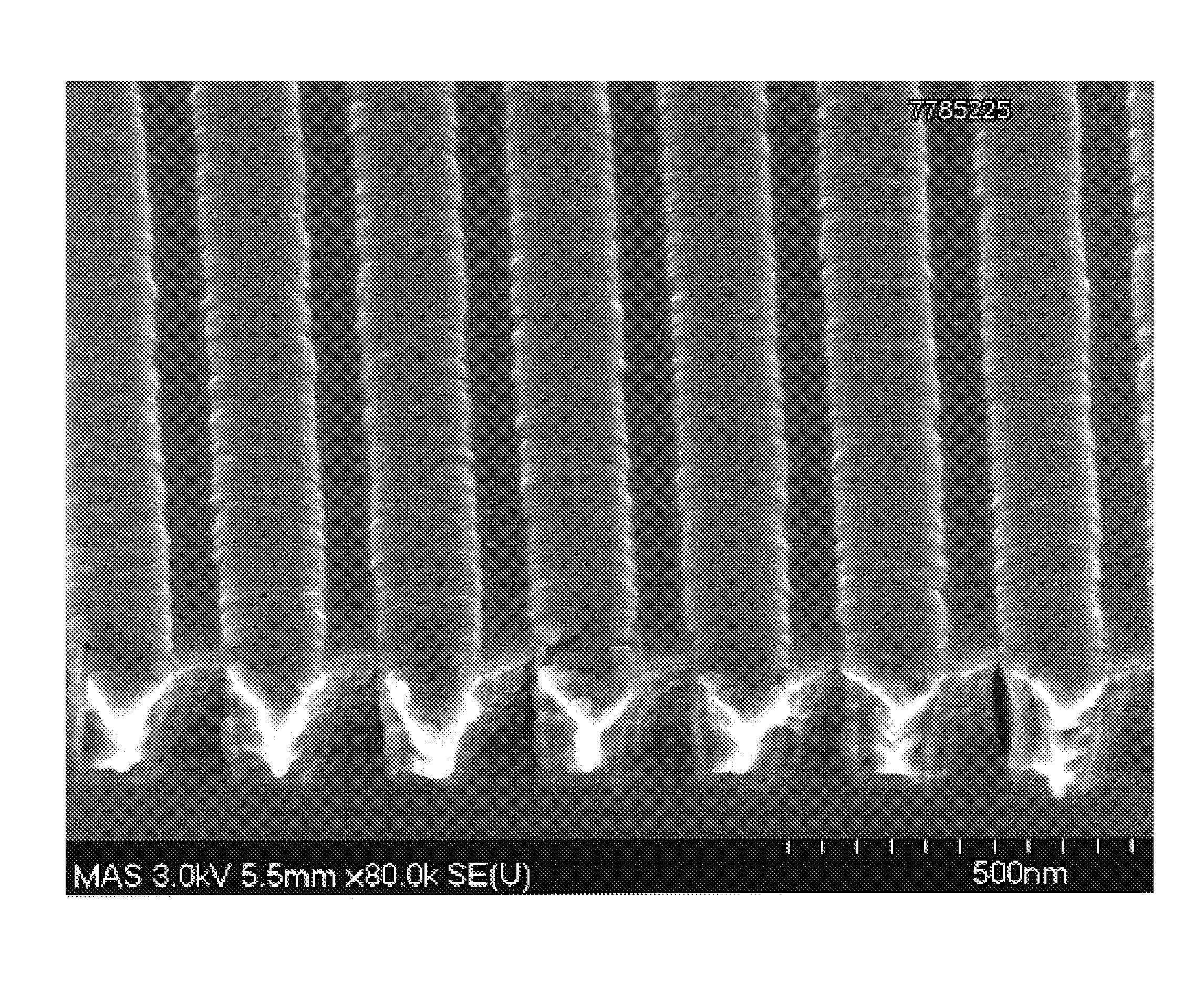
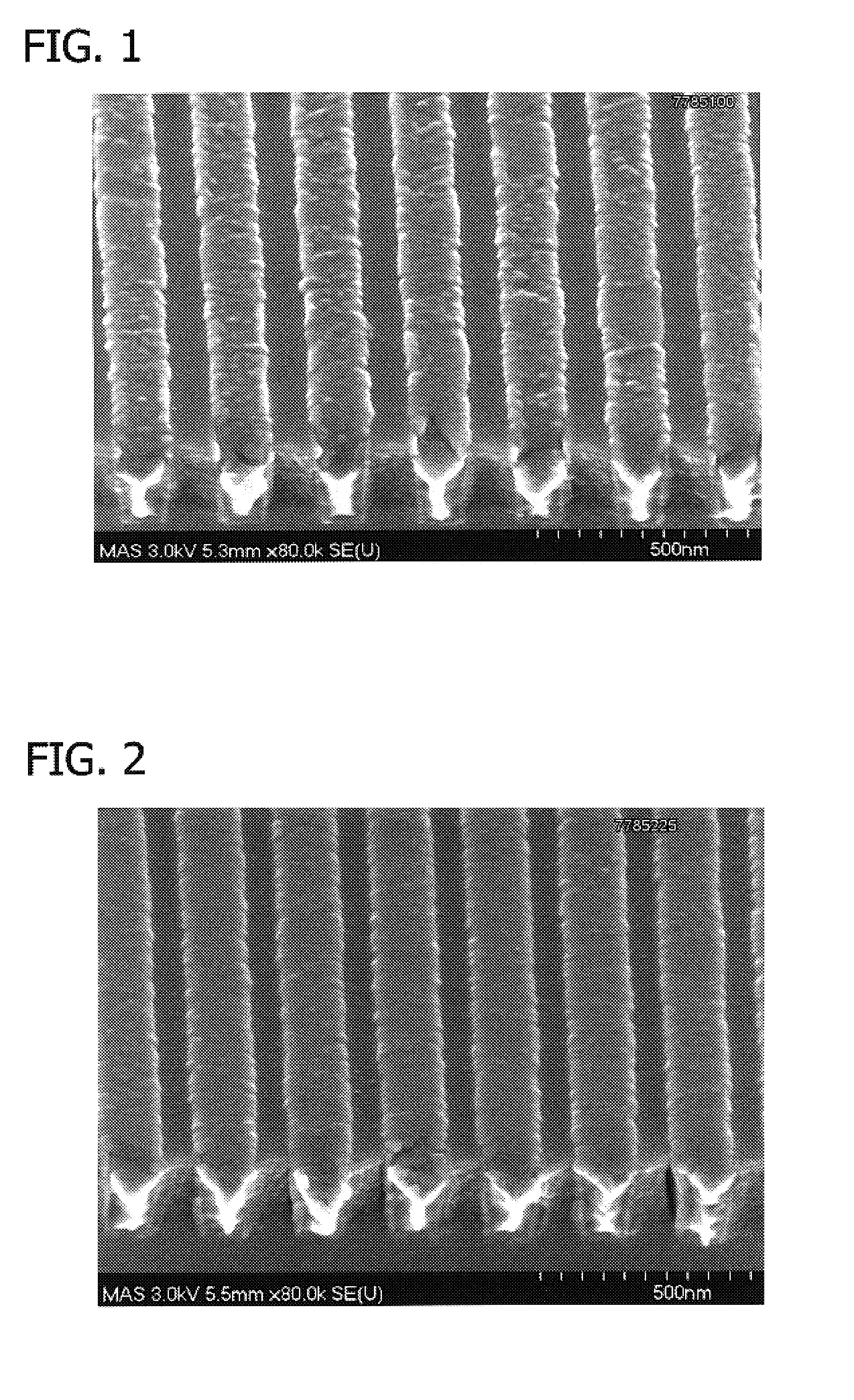
[0084]The difference in surface roughness achieved in a Co—W—P layer deposited from an electroless plating bath comprising a hydrazine-based leveling agent in accordance with the invention as compared to a plating bath without hydrazine can be seen by referring to FIGS. 1 and 2. FIGS. 1 and 2 are SEM photographs of Co—W—P capping layers at a magnification of 80,000×. The smooth surface of FIG. 2 exhibits the Co—W—P layer deposited in accordance with the present invention, i.e., a bath containing hydrazine. FIG. 1 exhibits the Co—W—P layer deposited by a plating bath that does not contain hydrazine.

[0085]A Co—W—P capping layer that exhibits the surface smoothness and planarity of the layer shown in FIG. 2 is smooth enough as deposited to function as a diffusion barrier layer over a Cu interconnect feature, with substantially reduced risk of electrical short either immediately after deposition or during the service life of the interconnect feature.

[0086]The Co—W—P capping layer of FIG...


PUM

PropertyMeasurementUnit
thicknessaaaaaaaaaa
surface roughnessaaaaaaaaaa
concentrationsaaaaaaaaaa

Abstract

An electroless plating method and composition for depositing Co, Ni, or alloys thereof onto a metal-based substrate in manufacture of microelectronic devices, involving a source of deposition ions selected from the group consisting of Co ions and Ni ions, a reducing agent for reducing the depositions ions to metal onto the substrate, and a hydrazine-based leveling agent.

Description

REFERENCE TO RELATED APPLICATION[0001]This application is based on provisional application Ser. No. 60 / 619,728, filed Oct. 18, 2004, which is incorporated herein by reference.FIELD OF THE INVENTION[0002]This invention relates to electroless plating of Co, Ni, and alloys thereof in microelectronic device applications.BACKGROUND OF THE INVENTION[0003]Electroless deposition of Co, Ni, and alloys thereof is employed in a variety of applications in the manufacture of microelectronic devices. For example, it is known to deposit a Co-based cap on interconnect metallization. In particular, in damascene processing, metallization is employed to form electrical interconnects in an integrated circuit substrate by metal-filling of interconnect features such as vias and trenches formed in the substrate.[0004]If metal deposited on an integrated circuit substrate is Cu, it can diffuse rapidly into the Si substrate and dielectric films such as, for example, SiO2 or low k dielectrics. Copper can also...

Claims


Application Information

Patent Timeline
Patent Type & Authority Patents(United States)
IPC IPC(8): C23C18/16C23C18/32C23C18/36
CPCC23C18/34C23C18/36C23C18/50H01L21/288H01L21/76849H05K3/244B05D1/18C09D5/00B05D5/12
Inventor VALVERDE, CHARLESPETROV, NICOLAIYAKOBSON, ERICCHEN, QINGYUNPANECCASIO, JR., VINCENTHURTUBISE, RICHARDWITT, CHRISTIAN
Owner MACDERMID ENTHONE INC
Learn More