Method for preventing the formation of a void in a bottom anti-reflective coating filling a via hole

a technology of anti-reflective coating and via hole, which is applied in the direction of photosensitive materials, instruments, photomechanical equipment, etc., can solve the problems of increased parasitic capacitance between interconnects on the same layer, increased resistance, delay of signal transfer,

Inactive Publication Date: 2008-02-26
DONGBU ELECTRONICS CO LTD
View PDF18 Cites 4 Cited by
  • Summary
  • Abstract
  • Description
  • Claims
  • Application Information

AI Technical Summary

Benefits of technology

[0016]Accordingly, the present invention has been made to solve the above-mentioned problems, and an object of the present invention is to provide a method for manufacturing a semiconductor device which, on performing a via first Dual Damascene process, inhibits or prevents the formation of a void in a bottom anti-reflective coating filling a via hole.
[0025]According to the present invention, the bottom anti-reflective coating (preferably comprising a novolac resin based mixture with a low glass transition temperature) is heated through a first heat treatment step to have excellent via filling ability and to reduce or prevent the formation of voids in the bottom anti-reflective coating. Therefore, the preferred BARC composition improves a planarization degree of the bottom anti-reflective coating. Also, the cross-link layer having an excellent chemical resistance is formed on the bottom anti-reflective coating by use of the acid diffusion material through a second heat treatment step so as to minimize a chemical reaction of the bottom anti-reflective coating with the photoresist in a subsequent photolithography process, thus improving a process reliability. Also, according to the present invention, the overall process time can be reduced and the investment for etching equipment can be minimized or curtailed, compared to conventional PR recess Dual Damascene processes.

Problems solved by technology

The narrowing of the interconnect generally causes an increase of resistance in the interconnect and furthermore a delay of signal transfer.
However, in the multi-layered interconnect structure, an interval (or spacing) between adjacent interconnect lines is further narrowed so that parasitic capacitance between interconnects on the same layer increases and signal transfer delay of the semiconductor device further increases.
However, in case of copper, since vapor pressure of certain etching by-products is low, it is generally difficult to dry etch copper.
Due to the void 107a formed in the BARC filling the via hole, in the subsequent trench formation process using the second photoresist pattern, a fence (indicated as 103a in FIG. 1D) may be formed, or a bottom face of the trench may not be uniformly etched, thereby deteriorating process reliability.
Also, according to the above-mentioned PR recess Dual Damascene method, since ashing of novolac resin and back side wet etching should be performed, the overall process is relatively complex and the process time becomes relatively long.

Method used


Image

  • Method for preventing the formation of a void in a bottom anti-reflective coating filling a via hole
  • Method for preventing the formation of a void in a bottom anti-reflective coating filling a via hole
  • Method for preventing the formation of a void in a bottom anti-reflective coating filling a via hole

Examples


Embodiment Construction

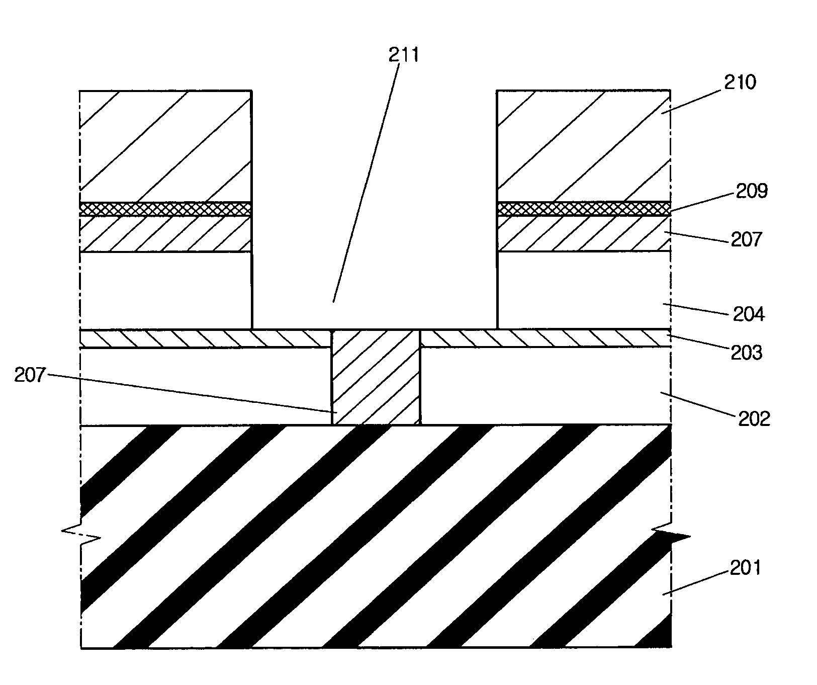
[0030]Hereinafter, a preferred embodiment of the present invention will be described with reference to the accompanying drawings. FIGS. 2A to 2F are cross-sectional views showing a method for manufacturing a semiconductor device according to a preferred embodiment of the present invention.

[0031]First, as shown in FIG. 2A, a first interlayer dielectric 202 with low permittivity is deposited on a semiconductor substrate 201. Herein, although not shown in the drawing, it is evident that on the semiconductor substrate, an isolation layer defining an active region of the substrate 201, a capacitor and / or a transistor on the active region, etc. may be previously formed.

[0032]The first interlayer dielectric 202 can be formed of various materials. In particular, a tetraethyl orthosilicate (TEOS)-based oxide layer (such as Low Pressure-TEOS, O3-TEOS, d-TEOS and so on), undoped silicate glass (USG), fluorosilicate glass (FSG), SiH4-based glass layer (e.g., deposited by High Density Plasma CVD...


PUM

PropertyMeasurementUnit
thicknessaaaaaaaaaa
temperatureaaaaaaaaaa

Abstract

A method for manufacturing a semiconductor device which, on performing a via first Dual Damascene process, inhibits or prevents the formation of a void in a bottom anti-reflective coating filling a via hole. The method typically includes the steps of forming a bottom anti-reflective coating (BARC) in a via hole in an interlayer dielectric on a semiconductor substrate sufficiently to fill the via hole; disposing an acid diffusion material on the BARC; forming a cross-link layer between the BARC and the acid diffusion material; removing the remaining acid diffusion material; and etching the cross-link layer, the BARC and the interlayer dielectric to form a trench extending from an upper portion of the via hole.

Description

BACKGROUND OF THE INVENTION[0001]1. Field of the Invention[0002]The present invention relates to a method for manufacturing a semiconductor device, and more particularly to a semiconductor device and method for manufacturing a semiconductor device which, on performing a “via first” Dual Damascene process, inhibits or prevents the formation of a void in a bottom anti-reflective coating filling a via hole.[0003]2. Description of the Background[0004]Generally, with the high integration of semiconductor devices, an interconnect becomes narrowed. The narrowing of the interconnect generally causes an increase of resistance in the interconnect and furthermore a delay of signal transfer. To solve the problem of signal transfer delay, a multi-layered interconnect structure has been introduced, generally replacing the previous single layered interconnect structure.[0005]However, in the multi-layered interconnect structure, an interval (or spacing) between adjacent interconnect lines is furthe...

Claims


Application Information

Patent Timeline
Patent Type & Authority Patents(United States)
IPC IPC(8): H01L21/4763G03F7/16H01L21/768H01L23/48H01L23/52H01L29/40
CPCH01L21/76808Y10S430/108G03F7/16
Inventor CHOI, YONG JUN
Owner DONGBU ELECTRONICS CO LTD
Why Eureka
Try Eureka