Method for etching high dielectric constant materials and for cleaning deposition chambers for high dielectric constant materials

a technology of high dielectric constant materials and deposition chambers, which is applied in the direction of cleaning hollow articles, energy-based chemical/physical/physico-chemical processes, coatings, etc., can solve the problems of high leakage current and device failure, no process details for plasma cleaning of ald chambers, and material electric breakdown of materials

Inactive Publication Date: 2008-04-15
VERSUM MATERIALS US LLC
View PDF35 Cites 400 Cited by
  • Summary
  • Abstract
  • Description
  • Claims
  • Application Information

AI Technical Summary

Benefits of technology

[0024]FIG. 3 provides a graphical illustration of the relative BCl3 plasma etch rates of various high dielectric constant materials, normalized to Al2O3.

Problems solved by technology

When the gate dielectric layer approaches thicknesses of a few nanometers or less, conventional SiO2, Si3N4, and SiON materials undergo electric breakdown and no longer provide insulation.
For example, crystallization of high-k materials such as HfO2 causes high leakage current and device failure.
However, no details of any process for plasma cleaning of ALD chambers were given in the above family of disclosures.
Again, these publications do not disclose any method to clean the ALD residues after the wafers have been processed.
Although the aforementioned high-k materials are excellent gate insulators, it is very difficult to dry etch these films for pattern transfer.
While the deposition process desirably generates high-k films on a substrate (typically a silicon wafer), the reactions that form these films also occur non-productively on other exposed surfaces inside of the deposition chamber.
Accumulation of deposition residues results in particle shedding, degradation of deposition uniformity, and processing drifts.
These effects can lead to wafer defects and subsequent device failure.
The authors also noted “Fairly similar trends were seen with BCl3 / Ar discharges, with the absolute rates being ˜20% lower than that for Cl2 / Ar.” While the authors' method may be used for anisotropic etching of flat panel display devices, high power plasma sputtering cannot be achieved on grounded chamber surfaces.
Therefore, the authors' methods cannot be extended to clean deposition residues within ALD chambers.
Such collimated ion beams cannot be used to clean deposition residues from ALD chambers.
However, mechanical cleaning methods are time-consuming, labor-intensive, and damaging to the surfaces being cleaned.
However, fluorine-based chemistry alone is ineffective to remove the high-k dielectric materials discussed above.
A, Vol. 17, pp 1326-1330, 1999, wherein the authors exposed Al2O3 coated wafers to NF3 / Ar based inductively coupled plasmas, and found that “the greater concentration of atomic F available at high source power contributed to thicker fluorinated surfaces, leading to the net deposition rather than etching.” In the case of high-k materials the metal fluoride product that forms is nonvolatile and, thus, difficult to remove from the reactor.

Method used


Image

  • Method for etching high dielectric constant materials and for cleaning deposition chambers for high dielectric constant materials
  • Method for etching high dielectric constant materials and for cleaning deposition chambers for high dielectric constant materials
  • Method for etching high dielectric constant materials and for cleaning deposition chambers for high dielectric constant materials

Examples


example 1

Plasma Etching / Cleaning of Al2O3 Samples

[0087]Since power is one of the key processing parameters in plasma etching / cleaning, we evaluated power dependence of Al2O3 etching by BCl3 plasma. The results are listed in Table 24 below.

[0088]

TABLE 24RF power dependence of Al2O3 etching by BCl3 plasmaPower densityPressureAl2O3 etch ratePower (W)(W / cm2)(mTorr)(nm / min)Vbias (V)500.275000.0161000.555003.0352001.105009.858

[0089]Apparently there is a threshold power density of 0.55 W / cm2 or threshold Vbias of 35 V for etching Al2O3. Higher power density and higher Vbias resulted in higher etch rate.

[0090]Next, we investigated chamber pressure dependence of Al2O3 etching by BCl3 plasma. The results are listed in Table 25 below.

[0091]

TABLE 25Chamber pressure dependence of Al2O3 etching by BCl3 plasmaPower densityPressureAl2O3 etch ratePower (W)(W / cm2)(mTorr)(nm / min)Vbias (V)1000.55507.2911000.555003.0351000.5510000.84

[0092]A higher etch rate was achieved at a reduced pressure. There are two facto...

example 2

Plasma Etching / Cleaning of HfO2 Samples

[0097]At 500 mTorr pressure, etching of HfO2 was achieved at all power levels between 50 and 200 W. The results are listed in Table 27 below.

[0098]

TABLE 27BCl3 plasma etching of HfO2Power densityPressureHfO2 etch ratePower (W)(W / cm2)(mTorr)(nm / min)Vbias (V)500.275001.614500.275001.4161000.555004.7342001.1050014.763

example 3

Plasma Etching / Cleaning of ZrO2 Samples

[0099]Several experiments were conducted with ZrO2 samples using 500 mTorr pressure and various power levels between 50 and 200 W. The results are listed in Table 28 below.

[0100]

TABLE 28BCl3 plasma etching of ZrO2Power densityPressureZrO2 etch ratePower (W)(W / cm2)(mTorr)(nm / min)Vbias (V)500.275000.3161000.55500−3.8*321000.55500−2.5*452001.105007.165*The film became thicker after one minute exposure to the plasma.

[0101]FIG. 3 shows the relative comparison of BCl3 plasma etch rates of high-k materials HfO2, Al2O3, and ZrO2 at 500 mTorr chamber pressure and 1 W / cm2 RF power density. It can be seen that HfO2 has the highest etch rate, and ZrO2 has the lowest etch rate among the three high-k materials.

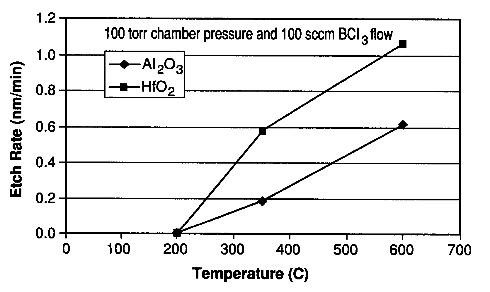
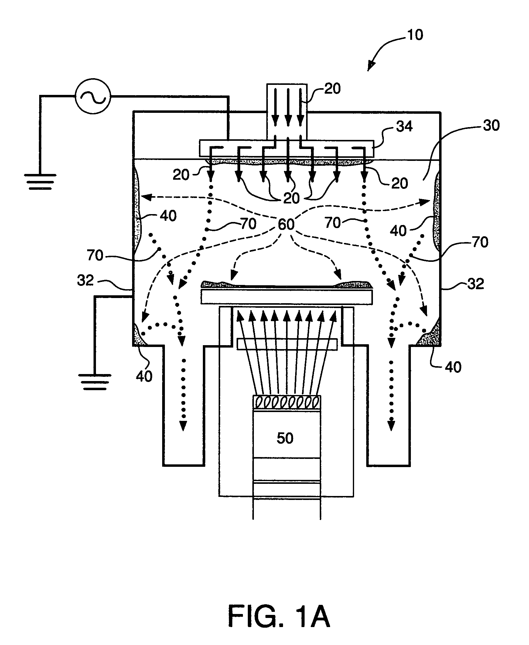
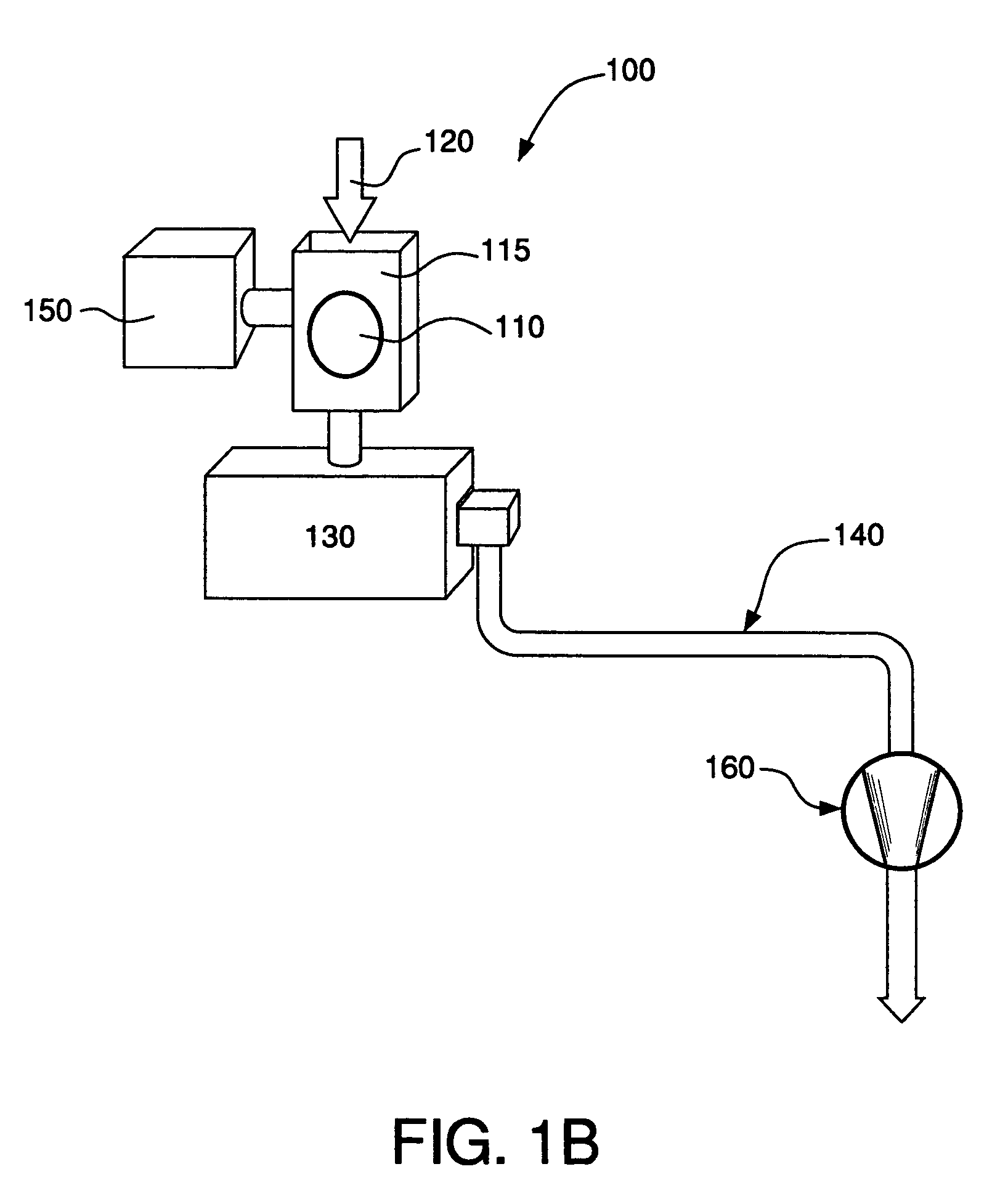
[0102]Examples 4 and 5 illustrate BCl3 thermal etching / cleaning of high-k materials. FIG. 4 is a schematic of the experimental setup for examples 4 and 5. In this reactor chamber 300, RF power 310 can be applied on the top electrode 320, and the lower ...


PUM

PropertyMeasurementUnit
dielectric constantaaaaaaaaaa
temperatureaaaaaaaaaa
pressureaaaaaaaaaa

Abstract

A process for the removal of a substance from a substrate for etching and/or cleaning applications is disclosed herein. In one embodiment, there is provided a process for removing a substance having a dielectric constant greater than silicon dioxide from a substrate by reacting the substance with a reactive agent that comprises at least one member from the group consisting a halogen-containing compound, a boron-containing compound, a hydrogen-containing compound, nitrogen-containing compound, a chelating compound, a carbon-containing compound, a chlorosilane, a hydrochlorosilane, or an organochlorosilane to form a volatile product and removing the volatile product from the substrate to thereby remove the substance from the substrate.

Description

CROSS-REFERENCE TO RELATED APPLICATIONS[0001]This application is a continuation-in-part of U.S. patent application Ser. No. 10 / 410,803, filed 10 Apr. 2003, which is a continuation-in-part of U.S. patent application Ser. No. 10 / 198,509, filed 18 Jul. 2002, now abandoned the disclosures of which are incorporated herein by reference in its entirety.BACKGROUND OF THE INVENTION[0002]In the manufacture of semiconductor integrated circuits (IC), dielectric materials such as silicon dioxide (SiO2), silicon nitride (Si3N4), and silicon oxynitride (SiON) have been widely used as insulators for transistor gates. Such insulators are often called gate dielectrics. As IC device geometry shrinks, gate dielectric layers have become progressively thinner. When the gate dielectric layer approaches thicknesses of a few nanometers or less, conventional SiO2, Si3N4, and SiON materials undergo electric breakdown and no longer provide insulation. To maintain adequate breakdown voltage at very small thickn...

Claims


Application Information

Patent Timeline
Patent Type & Authority Patents(United States)
IPC IPC(8): B08B9/00B08B6/00B01J19/08B08B7/00C23C16/44H01L21/20H01L21/304H01L21/306H01L21/3065H01L21/31
CPCB08B7/00B08B7/0035C23C16/4405H01L21/3065H01L21/20
Inventor JI, BINGMOTIKA, STEPHEN ANDREWPEARLSTEIN, RONALD MARTINKARWACKI, JR., EUGENE JOSEPHWU, DINGJUN
Owner VERSUM MATERIALS US LLC
Why Eureka
Try Eureka