System and method for cutting using a variable astigmatic focal beam spot

a technology of astigmatic focal beam and cutting system, which is applied in the field of laser cutting or machining, can solve the problems of low die yield, high operating cost, and low throughpu

Active Publication Date: 2008-06-17
IPG PHOTONICS CORP
View PDF100 Cites 48 Cited by
  • Summary
  • Abstract
  • Description
  • Claims
  • Application Information

AI Technical Summary

Benefits of technology

[0021]According to yet another aspect of the present invention, a method is provided for scribing a sapphire substrate having a layer of GaN. This method comprises directing pulses of laser energy forming an astigmatic focal beam spot at a surface of the GaN on th

Problems solved by technology

The extreme hardness of blue LED substrates and the small LED die size create significant problems for both saw dicing and mechanical scribing, including low die yield, low throughput, and high operating costs.
The brittle substrates, such as GaP and GaAs, also show low productivity due to excessive edge chipping by the mechanical scribe and break and the saw dicing processes.
Moreover, the conventional processes require relatively large cutting areas, reducing the number of devices on a wafer.
Although coupling of a UV laser at 266 nm is efficient on these substrates, excessive photonic energy under this strong absorption can result in unnecessary thermal conduction to the substrates, causing heat related damages.
In contrast, insufficient laser energy density can result in improper ablation, even with the strong absorption.
Thus, introducing the mask in a beam delivery system (BDS) blocks a major portion of the laser beam, which makes the beam utilization factor (BUF) low.
This low beam utilization factor limits the speed of the scribing process, because the scribing speed is mainly proportional to the size of the projected beam in the scribing translation

Method used


Image

  • System and method for cutting using a variable astigmatic focal beam spot
  • System and method for cutting using a variable astigmatic focal beam spot
  • System and method for cutting using a variable astigmatic focal beam spot

Examples


Embodiment Construction

Overview of BDS

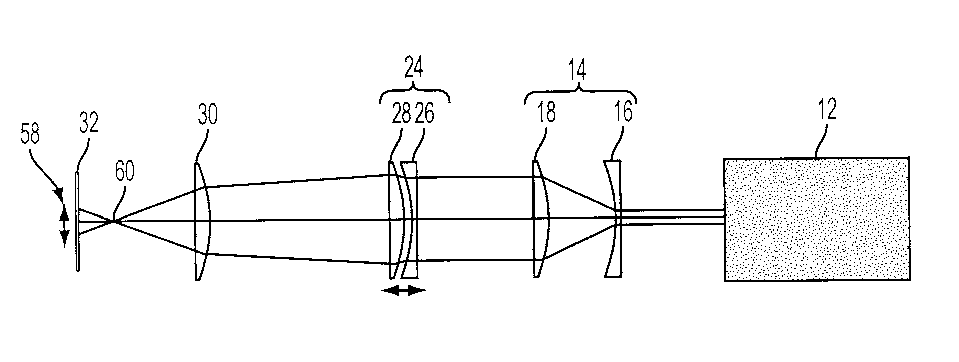
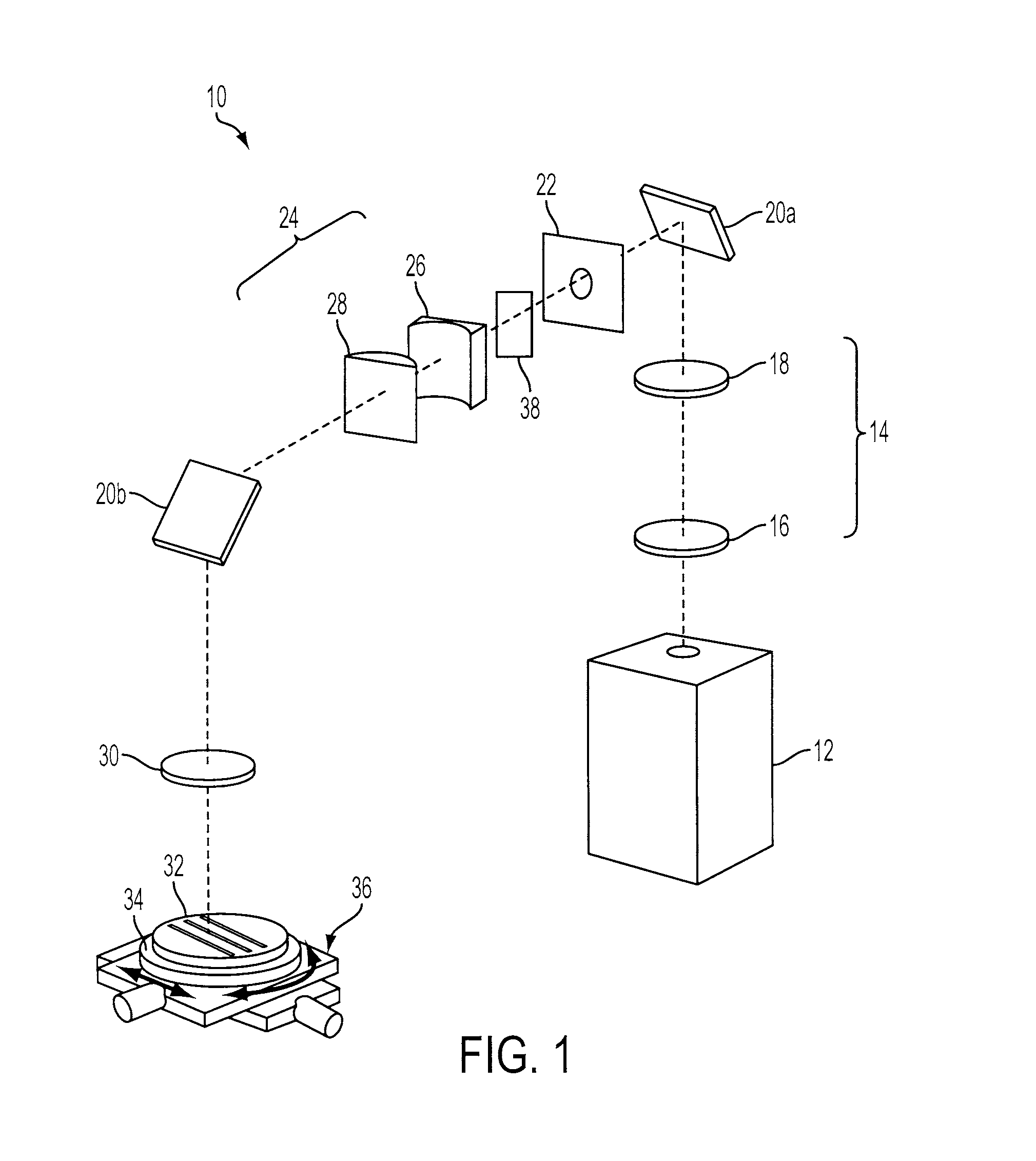
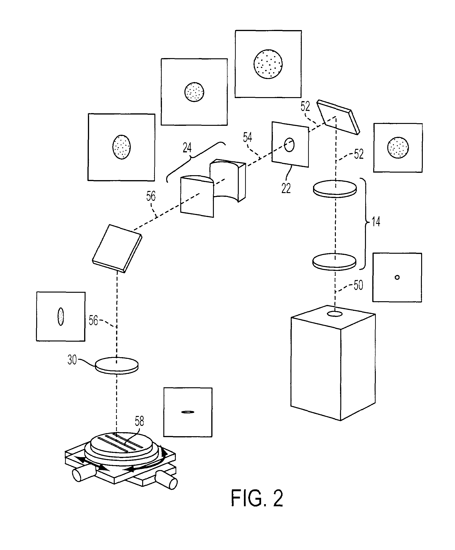
[0038]Referring to FIG. 1, one embodiment of an anamorphic beam delivery system (BDS) 10 is described in detail. The anamorphic BDS 10 generates an astigmatic focal beam spot that can be used to cut or machine a substrate made of various types of materials. In one exemplary application, the preferred embodiment of the BDS 10 improves the productivity of LED die separation by forming a highly-resolved adjustable astigmatic focal beam spot, which maximizes scribing speed and minimizes consumption of scribing-related real estate on a wafer. The BDS 10 can also be used in other scribing or cutting applications.

[0039]In the embodiment shown, a solid-state laser 12, preferably diode pumped, generates a laser beam in the UV range, preferably the third harmonic 355 nm or the fourth harmonic 266 nm. The raw laser beam is usually in TEM00 mode with Gaussian distribution and is enlarged by a beam-expanding telescope (BET) 14. The exemplary embodiment of the BET 14 is composed of...


PUM

PropertyMeasurementUnit
Angleaaaaaaaaaa
Widthaaaaaaaaaa
Widthaaaaaaaaaa

Abstract

A variable astigmatic focal beam spot is formed using lasers with an anamorphic beam delivery system. The variable astigmatic focal beam spot can be used for cutting applications, for example, to scribe semiconductor wafers such as light emitting diode (LED) wafers. The exemplary anamorphic beam delivery system comprises a series of optical components, which deliberately introduce astigmatism to produce focal points separated into two principal meridians, i.e. vertical and horizontal. The astigmatic focal points result in an asymmetric, yet sharply focused, beam spot that consists of sharpened leading and trailing edges. Adjusting the astigmatic focal points changes the aspect ratio of the compressed focal beam spot, allowing adjustment of energy density at the target without affecting laser output power. Scribing wafers with properly optimized energy and power density increases scribing speeds while minimizing excessive heating and collateral material damage.

Description

CROSS-REFERENCE TO RELATED APPLICATIONS[0001]This application claims the benefit of co-pending U.S. Provisional Patent Application Ser. No. 60 / 448,503, filed on Feb. 19, 2003, which is fully incorporated herein by reference.TECHNICAL FIELD[0002]This invention relates to laser cutting or machining, and more particularly, relates to a system and method for forming a variable astigmatic focal beam spot using solid-state lasers with an anamorphic beam delivery system to scribe semiconductor wafers.BACKGROUND INFORMATION[0003]Increasing worldwide demand for compound semiconductor devices has driven the development of high throughput, cost effective, and reliable production techniques and equipment. Compound semiconductors are comprised of a combination of group-III elements, such as B, Al, Ga, In and Ti, and group-V elements, such as N, P, As, Sb and Bi. A typical example of III-V compound semiconductor devices is light emitting diodes (LEDs) using InP, GaP, GaAs, AlInGaP and GaN.[0004]A...

Claims


Application Information

Patent Timeline
IPC IPC(8): B23K26/00B23K26/06B23K26/067B23K26/073B23K26/40G02B3/00G02B9/00G02B13/08G03F7/20
CPCB23K26/0608B23K26/0613B23K26/0617B23K26/0635B23K26/0656B23K26/067G03F7/70383B23K26/367B23K26/407B23K26/4075B23K26/0736B23K2201/40B23K2203/12B23K26/364B23K26/0624B23K26/066B23K26/40B23K2101/40B23K2103/12B23K2103/50H01L21/78H01L21/268
Inventor SERCEL, PATRICK J.SERCEL, JEFFREY P.PARK, JONGKOOK
Owner IPG PHOTONICS CORP
Why Eureka
Try Eureka