Electrochromic device

a technology of electrochromic layer and electrode, applied in non-linear optics, instruments, optics, etc., can solve the problems of high power consumption, inability to obtain color density corresponding to the thickness of the electrochromic layer, and inability to easily achieve color density. , to achieve the effect of improving color density, simple structure and small thickness

Inactive Publication Date: 2008-07-08
HITACHI LTD
View PDF11 Cites 12 Cited by
  • Summary
  • Abstract
  • Description
  • Claims
  • Application Information

AI Technical Summary

Benefits of technology

[0014]Although the electrochromic device having the structure shown in FIG. 31 has the advantage that, since oxidation and reduction take place simultaneously at two electrochromic layers which are respectively in contact with a pair of electrodes, the electrochromic reaction rate and efficiency are high, and a high coloring contrast is obtained. On the other hand, the light transmittance of the device decreased overall.
[0018]According to the invention, an electrochromic device and electrochromic apparatus of simple structure and small thickness can be obtained. An information recording medium having superior repeat coloration properties and high light transmittance, and a recording / reproducing method and a recording / reproducing device using this medium, are thereby obtained.

Problems solved by technology

However, in Type A wherein an electrochromic layer is provided in contact with a substrate having plural electrodes, and an electrolyte layer is formed on the electrochromic layer, since there were many electric current components which penetrate only the electrochromic layer which has a relatively low resistance, the power consumption was high.
Also, with any of these in-plane switching electrochromic devices, since the potential slope of the electric field which generates the coloring when a voltage is applied, arises from the interface which advances towards the electrochromic layer from the electrolyte layer, coloration does not occur easily at the electrochromic layer which is far from the interface in a perpendicular direction, and the coloring density corresponding to the thickness of the electrochromic layer is not obtained.

Method used


Image

  • Electrochromic device
  • Electrochromic device
  • Electrochromic device

Examples


example 1

(Construction and Manufacture)

[0080]FIG. 11 is a diagram showing a process for manufacturing the electrochromic device of the invention according to a first method.

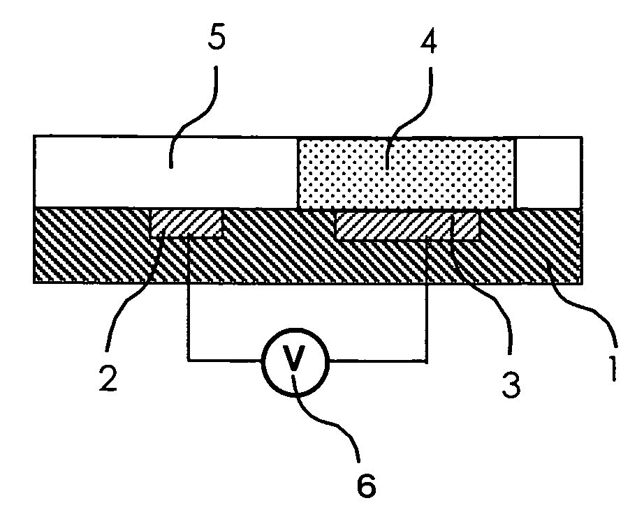
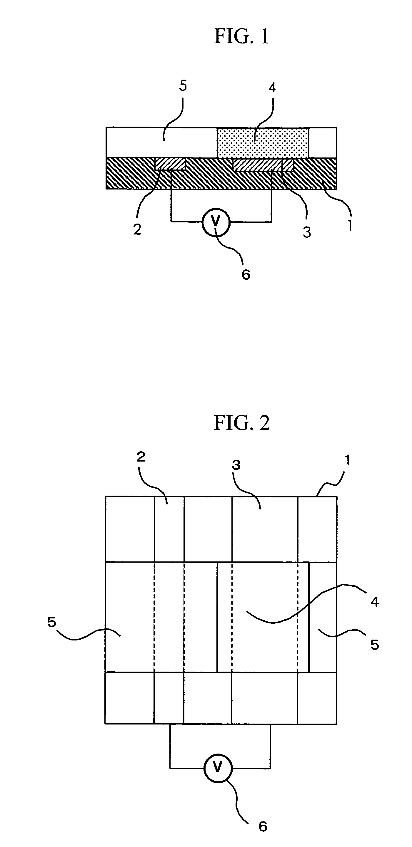
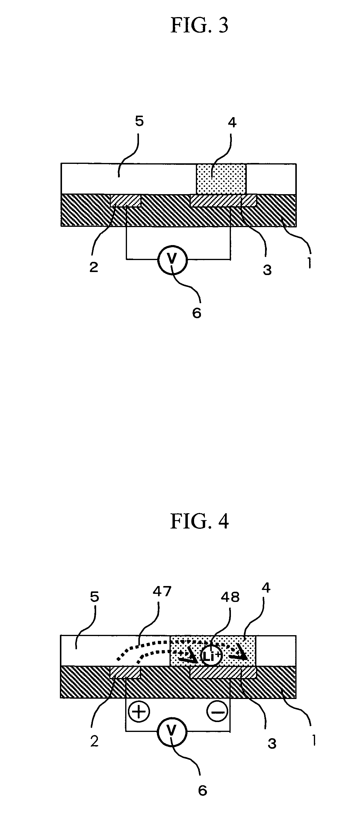
[0081]A 150 nm thick electrochromic layer 366 of a poly(3,4-ethylene dioxythiophene)-polystyrene sulfonic acid complex was formed by a photolithography process on a 3 cm square, 1 mm thick insulating glass substrate 361 carrying an ITO electrode 363 and an ITO electrode 364 of width 5 mm and thickness 50 nm.

[0082]A solution of composition 20 wt % polyethylene oxide having a molecular weight of 1 million, 2 wt % lithium perchlorate and 78 wt % tetrahydrofuran was then spin-coated on the remaining exposed part of the substrate at 1000 rpm for 60 seconds to form a 150 nm thick electrolyte layer 368, and an electrochromic device was thus produced.

(Operation of Electrochromic Device)

[0083]FIG. 12 is a diagram of the produced device viewed from the upper part of the electrolyte layer. When a voltage of 6V was applied to the fir...

example 2

[0094]An electrochromic device having the first structure according to the invention was manufactured in exactly the same way as in Example 1, except that tungstic oxide was used for the electrochromic compound, and a photolithography process and RF magnetron sputtering were used to form the electrochromic layer. When this device was connected to a power supply as in Example 1 and a voltage was applied between the electrodes, reversible coloring could be performed.

[0095]If the device was manufactured using iridium oxide, nickel oxide, titanium oxide or vanadium pentoxide for the electrochromic compound, reversible coloring could still be performed.

example 3

[0096]This example relates to a device panel wherein the pixels in the electrochromic device of the invention are arranged in a matrix, and to an information display using same.

[0097]A matrix display panel and device using 12 electrochromic devices, which are shown in FIGS. 15 and 16, were manufactured by the following methods. The materials used are the same as those of Example 1. FIG. 15 shows the construction of the display panel and FIG. 16 shows the construction of the information display.

[0098]A silicon thin film is formed on a substrate 463, an integrated circuit comprising a pixel driver region 464, buffer amplifier 465 and gate driver region 466 is provided thereupon, and the whole is connected to an image information display panel 461 comprising pixels 462. 467 is a shift register region and 468 is a data driver region.

[0099]The method of manufacturing the display panel is as follows.

[0100]A signal wire 439 and gate line 440 were manufactured on a glass substrate. Next, 12...


PUM

PropertyMeasurementUnit
distanceaaaaaaaaaa
thicknessaaaaaaaaaa
ion conductivityaaaaaaaaaa

Abstract

This invention provides an electrochromic device which has superior coloration repeat properties, high light transmittance and small thickness. A film is provided comprising a first electrode and second electrode in the same plane, and an electrochromic region and electrolyte region laminated in this plane. The electrochromic region is provided on the second electrode, the electrolyte region is provided on the first electrode, and the boundary between the electrochromic region and electrolyte region lies in the planar direction of the film.

Description

CLAIM OF PRIORITY[0001]The present application claims priority from Japanese application JP-A No. 146957 / 2005 filed on May 19, 2005, the content of which is hereby incorporated by reference into this application.CROSS REFERENCE TO RELATED APPLICATION[0002]U.S. patent application Ser. Nos. 10 / 998,653, 10 / 928,284 and 11 / 147,271 are co-pending applications of this application. The content of which are incorporated herein by cross-reference.FIELD OF THE INVENTION[0003]This invention relates to an electrochromic device which operates using the principle of electrochromism.BACKGROUND OF THE INVENTION[0004]“Electrochromism”, a phenomenon wherein the color of a compound changes reversibly with the application of a voltage, has been applied to modulated light window and display devices. In a prior art electrochromic device, an electrochromic layer and electrolyte layer are sandwiched between a pair of electrodes in which at least one is a transparent electrode, and electrochromism is manifes...

Claims


Application Information

Patent Timeline
Patent Type & Authority Patents(United States)
IPC IPC(8): G02F1/153
CPCG02F1/155G02F2001/1557
Inventor KOJIMA, KYOKO
Owner HITACHI LTD
Why Eureka
Try Eureka