Laser irradiation apparatus and method of manufacturing semiconductor device

a laser beam and semiconductor technology, applied in metal working apparatus, manufacturing tools, transistors, etc., can solve the problems of inferior heat resistance of glass substrates and inability to irradiate semiconductor films in uniform manner with laser beams, and achieve the effect of efficient and uniform radiation

Inactive Publication Date: 2008-07-29
SEMICON ENERGY LAB CO LTD
View PDF50 Cites 16 Cited by
  • Summary
  • Abstract
  • Description
  • Claims
  • Application Information

AI Technical Summary

Benefits of technology

[0013]In view of the problems mentioned above, it is an object of the present invention to provide a continuous wave laser irradiation apparatus and to provide a pulsed laser irradiation apparatus, in which a surface of an object is irradiated with a laser beam efficiently and uniformly. Further, it is another object to provide a method of manufacturing a semiconductor device by using the laser irradiation apparatus.
[0016]In other words, the laser irradiation apparatus of the present invention having a galvanometer mirror and an f-θ lens optical system, can offset the change of the energy due to the transmittance change of the f-θ lens, and can scan a laser beam while the fluctuation of the energy on a substrate is suppressed (an object to be irradiated).
[0017]A beam is scanned by a galvanometer mirror. Generally, the energy is, however, highest in the vicinity of the center of the substrate, and the energy becomes attenuated toward the edges of the substrate due to the difference in the transmittance of the lens. And the transmittance of the lens changes continuously by location, so that the energy of the transmitted beam also changes continuously. Therefore, the energy of the laser beam that is incident on the lens is controlled in advance by combining the optical system changing the branching ratio of polarization of the laser beam and the optical system having polarization dependency on the laser beam and changed continuously according to the transmittance of the position of the lens on which the laser beam is incident. It is noted that the branching ratio of polarization described here means a ratio of a maximum amplitude of a p-polarized light component to a maximum amplitude of a s-polarized light component in resolution of an electric field vector of polarized light into a p-polarization direction and a s-polarization direction. The laser energy is controlled to offset the transmittance of the lens, and thereby energy fluctuation in the laser beam irradiation of the substrate can be prevented.
[0018]By the laser irradiation apparatus of the present invention above, an object can be irradiated with the laser beam at high speed. In addition, the whole surface of a substrate can be crystallized uniformly.

Problems solved by technology

However, a glass substrate is inferior in heat resistance and the shape thereof is changed easily by heating.
However, since the f-θ lens used as a means for converging a laser beam has different transmittance in the center and in the edge of the lens, when the f-θ lens is used for laser crystallization the energy distribution of the laser beam irradiation of the semiconductor film is not uniform and thus, the whole semiconductor film cannot be irradiated uniformly with the laser beam.

Method used


Image

  • Laser irradiation apparatus and method of manufacturing semiconductor device
  • Laser irradiation apparatus and method of manufacturing semiconductor device
  • Laser irradiation apparatus and method of manufacturing semiconductor device

Examples


embodiment 1

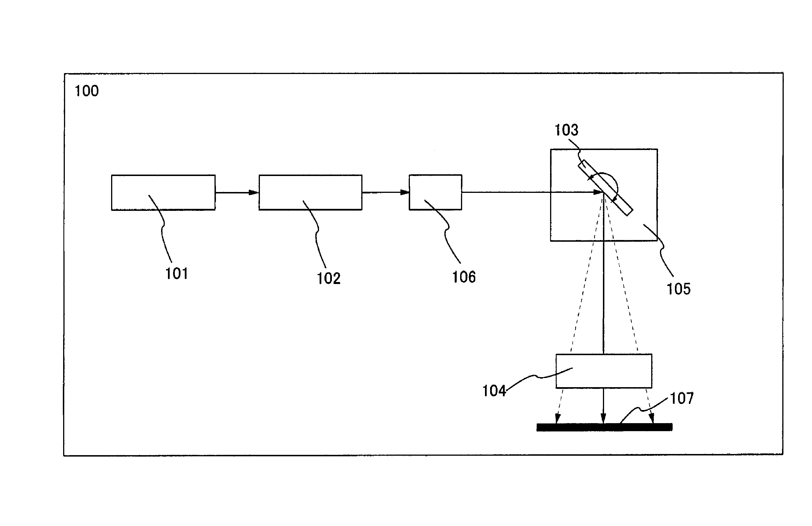
[0044]This embodiment describes a structure in which a half-wave plate and a beam splitter are interposed between an optical system for shaping a beam and a galvanometer mirror.

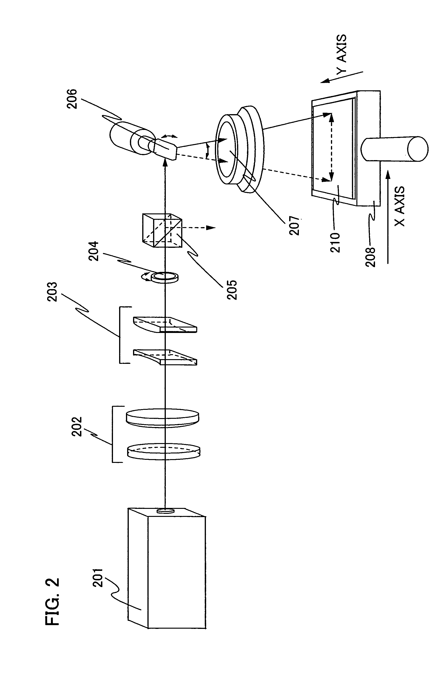
[0045]FIG. 2 shows an example of a laser irradiation apparatus. The description given here is about a case in which a laser beam emitted from a laser oscillator 201 is linearly p-polarized light beam (light beam is hereinafter referred to as beam) according to the polarization characteristic of the laser. A laser beam emitted from the laser oscillator 201 is shaped into a linear beam by a beam expander 202 and a cylindrical lens 203.

[0046]The shaped beam enters a half-wave plate 204. The half-wave plate 204 rotates about the normal line that runs in the center of the incident plane, thereby changing the branching ratio of polarization of the laser beam. In this way, the ratio of p-polarized laser beam in transmitted beam from the half-wave plate 204 can be increased or decreased.

[0047]The laser beam that has ...

embodiment 2

[0054]The case in which the scanning of the laser beam shown in the embodiment 1 is performed by controlling a galvanometer mirror in both X axis and Y axis directions is described in this embodiment.

[0055]The energy of the laser beam scanned depending on the change of a transmittance is changed, since the transmittance of the f-θ lens in the apparatus changed by location. FIGS. 6A and 6B shows an example of an irradiation energy change of the laser beam scanned on a substrate. FIGS. 6A and 6B shows that laser intensity around the center of a substrate is high, while the laser intensity becomes lower concentrically from the center toward edges of the substrate. Accordingly, around the center of the substrate in which the transmittance of the lens is high, the irradiation energy change on the substrate can be suppressed by controlling the rotation of a half-wave plate so that intensity of the beam transmitted from a beam splitter can be reduced.

[0056]FIGS. 7A and 7B shows an example ...

embodiment 3

[0059]This embodiment describes a structure in which the half-wave plate is interposed between the optical system for shaping a beam and the galvanometer mirror.

[0060]A case in which a laser beam emitted from a laser oscillator is linearly polarized is described. Given here as an example is a case of using a laser whose polarization characteristics cause p-polarization.

[0061]A laser beam emitted from the laser oscillator is shaped by an optical system. The shaped beam enters the half-wave plate. The half-wave plate rotates around the axis that is the normal line of the half-wave plate, thereby changing the branching ratio of polarization of the incident beam. In this way, the ratio of p-polarized beam in incident beam can be increased or decreased. When the laser beam enters the half-wave plate in a manner that positions the oscillation direction of the incident beam in parallel to the optical axis direction of the half-wave plate, the laser beam, which is p-polarized beam, is trans...


PUM

PropertyMeasurementUnit
transmittanceaaaaaaaaaa
angleaaaaaaaaaa

Abstract

The present invention provides the laser irradiation apparatus that has a galvanometer mirror and an f-θ lens optical system, can offset the change of the energy due to the transmittance change of the f-θ lens, and can scan a laser beam while the change of the energy on a substrate is suppressed. Further, the laser beam energy that is incident on the lens is controlled in advance by combining the optical system changing the branching ratio of polarization of the laser beam and the optical system having dependence on direction of polarization of the laser beam and changed continuously according to the transmittance of the lens on which the laser beam is incident. The laser energy is controlled to offset the transmittance of the lens, and thereby energy fluctuation of the laser beam irradiation of a substrate can be prevented.

Description

BACKGROUND OF THE INVENTION[0001]1. Field of the Invention[0002]The present invention relates to a laser irradiation apparatus for crystallizing a semiconductor film and the like or for activating the semiconductor film after ion implantation by using a laser beam. Specifically, the present invention relates to a laser irradiation apparatus for irradiating the laser beam on a semiconductor film which is polycrystalline or similar to polycrystalline and enhancing crystallinity of the semiconductor film. Further, the present invention relates to a method of manufacturing semiconductor device using a crystalline semiconductor film formed by the laser irradiation apparatus.[0003]2. Description of the Related Art[0004]In recent years, the technology for forming a thin film transistor (TFT) over a substrate has made great progress and such a TFT has been developed and applied to an active matrix semiconductor device. Particularly, a TFT made by using a polycrystalline semiconductor film i...

Claims


Application Information

Patent Timeline
Patent Type & Authority Patents(United States)
IPC IPC(8): H01L21/00H01L21/84B23K26/073B23K26/08H01L21/20H01L21/268H01L21/3213H01L21/77H01L27/12H01L29/04H01L29/786
CPCB23K26/0736B23K26/0738B23K26/08B23K26/0807B23K26/0815H01L27/1285H01L21/268H01L21/32136H01L27/12H01L29/78675H01L21/2026B23K2201/40H01L29/04B23K26/0821B23K26/082B23K2101/40H01L21/02425H01L21/02686H01L21/02683H01L21/02502H01L21/02678H01L21/02488H01L21/02422H01L21/02532H01L21/0242H01L21/02691
Inventor OISHI, HIROTADA
Owner SEMICON ENERGY LAB CO LTD
Why Eureka
Try Eureka