Contact structure and semiconductor device

Inactive Publication Date: 2008-08-12
SEMICON ENERGY LAB CO LTD
View PDF42 Cites 45 Cited by
  • Summary
  • Abstract
  • Description
  • Claims
  • Application Information

AI Technical Summary

Benefits of technology

[0015]Still further, according to another aspect of the present invention, there is provided a semiconductor device comprising a first substrate having a circuit structured with a thin film transistor and a second substrate opposing the first substrate, characterized in that a connecting wiring formed of a metallic film and a transparent conductive film in contact with the metallic film surfa

Problems solved by technology

The TFT using the amorphous silicon film as the active layer essentially cannot attain an electric field effect mobility of several cm2/Vsec or more because of electronic properties caused by the amorphous structure, or the like.
Accordingly, despite being able to utilize the TFT as the switching element (pixel TFT) for driving the liquid crystals provided in each pixel in the pixel portion, it is impossible t

Method used


Image

  • Contact structure and semiconductor device
  • Contact structure and semiconductor device
  • Contact structure and semiconductor device

Examples


embodiment mode 1

[0047]A contact structure according to the present invention is suitable for a semiconductor device that uses a mounting method in which circuits are connected by means of an anisotropic conductive film, such as an active matrix type liquid crystal display device or an EL display device. Referring to FIGS. 12A and 12B, the contact structure of the present invention when applied to the active matrix type liquid crystal display device is described in Embodiment Mode 1.

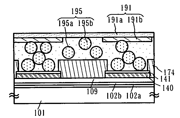
[0048]A connecting wiring 183 on an active matrix substrate is electrically connected to an FPC 191 by an anisotropic conductive film 195 in a terminal portion 182. The connecting wiring 183 is formed in the same process in which a source / drain wiring of a TFT on the active matrix substrate is formed. In other words, the connecting wiring 183 is formed from the same material and in the same layer as that of the source / drain wiring. The connecting wiring 183 is a lamination film of a metallic film 140 and a transparent co...

embodiment mode 2

[0054]Further, for the case of forming the connecting wiring in the same process with the gate wiring, the shape of the sectional surfaces of the gate wiring and the connecting wiring can be taper shapes. By forming the gating wiring into a taper shape, film thickness is reduced from the center towards the side surface. Because of this variation in film thickness, as shown in an embodiment which will be explained later, changing an impurity concentration to be doped into the semiconductor film can be made by utilizing the variation in film thickness in a process of doping for the semiconductor film with the gate wiring as a mask.

[0055]Dry etching utilizing high-density plasma is applied in order to form a taper shaped gate wiring. As a means of achieving high-density plasma, an etching device that utilizes a microwave or an ICP (Inductively Coupled Plasma) is suitable. Particularly, the ICP etching device can easily control plasma as well as deal with the operation of processing for...

embodiment 1

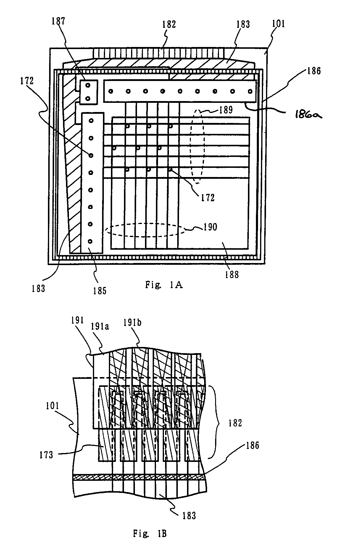
[0072]This Embodiment relates to an active matrix type liquid crystal panel. FIG. 1A is a diagram showing the top view of the active matrix substrate of this Embodiment in which a pixel portion and a driver circuit for driving the thin film transistor of the pixel portion are formed thereon, and also shows the positional relationship between a column-shape spacer formed on the active matrix substrate and a sealing agent.

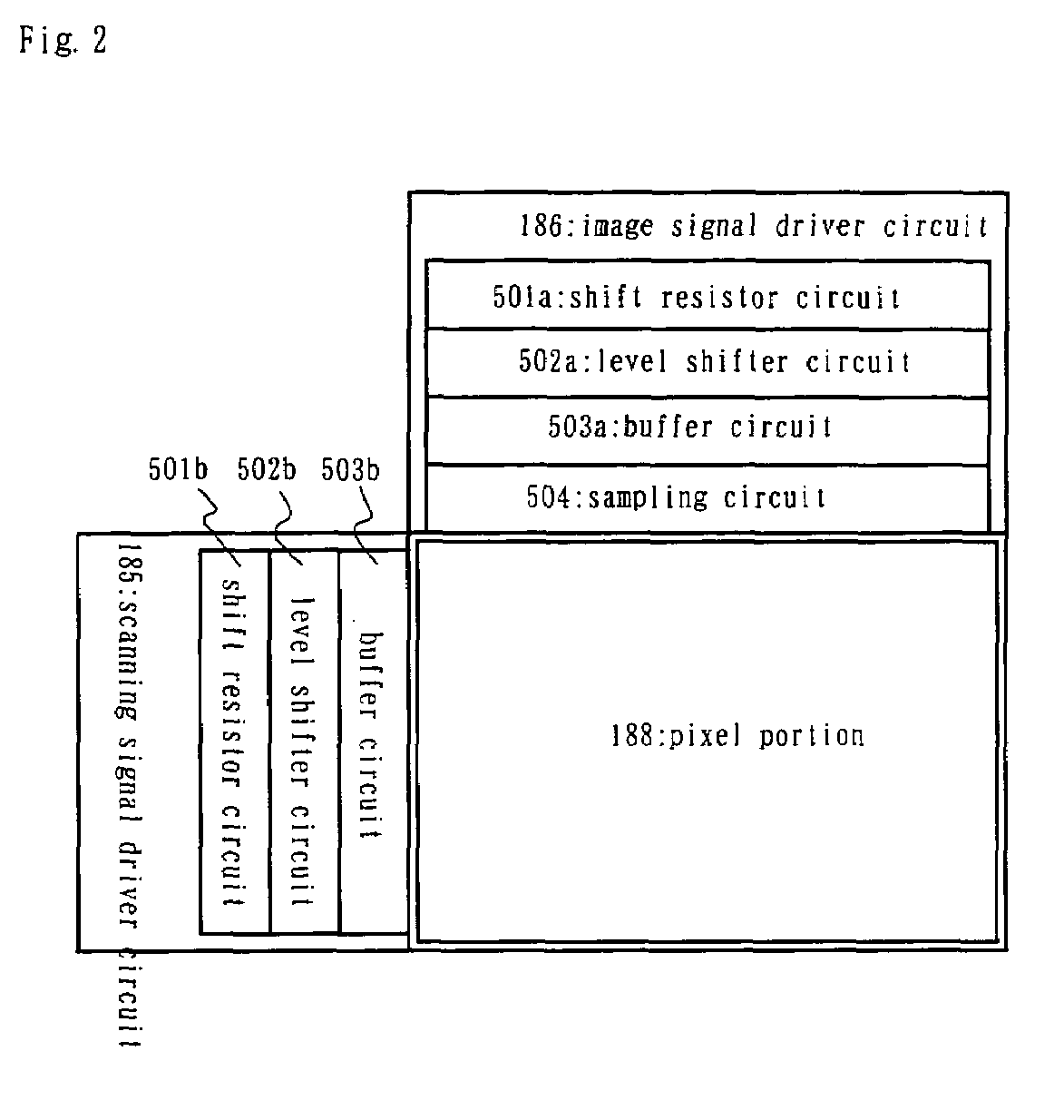
[0073]As shown in FIG. 1A, on a glass substrate 101, there are provided a pixel portion 188 disposed with a thin film transistor, a scanning signal driver circuit 185, and an image signal driver circuit 186a as the driver circuit for driving the thin film transistor disposed in the pixel portion. In addition, a signal processing circuit 187 such as a CPU or a memory circuit is provided.

[0074]In the pixel portion 188, a gate wiring 189 extending from the scanning signal driver circuit 185 and a source wiring 190 extending from the image signal driver circuit 186a inte...


PUM


Abstract

To improve the reliability of contact with an anisotropic conductive film in a semiconductor device such as a liquid crystal display panel, a terminal portion (182) of a connecting wiring (183) on an active matrix substrate is electrically connected to an FPC (191) by an anisotropic conductive film (195). The connecting wiring (183) is manufactured in the same process with a source/drain wiring of a TFT on the active matrix substrate, and is made of a lamination film of a metallic film and a transparent conductive film. In the connecting portion with the anisotropic conductive film (195), a side surface of the connecting wiring (183) is covered with a protecting film (173) made of an insulating material. Accordingly, the portion in which the metallic film is surrounded by the transparent conductive film, the insulating base film, and the protecting film (173) to which it is in contact with, can be avoided from exposure to air because the side surface of the metallic film of the connecting wiring is covered with the protecting film (173).

Description

BACKGROUND OF THE INVENTION[0001]1. Field of the Invention[0002]The present invention relates to a semiconductor device comprising a circuit structured with a thin film transistor (hereinafter referred to as TFT) formed on a substrate having an insulating surface, and also relates to a structure of a terminal for connecting the circuit structured with the TFT to a circuit on another substrate. More particularly, the present invention provides a technique suitable for use in a liquid crystal display device having a pixel portion and a driver circuit provided in the periphery of the pixel portion on the same substrate, an electro-luminescence display device, and electronic equipment mounted with an electro-optical device incorporating the above display devices. Note that in the present specification, the semiconductor device indicates general devices that may function by use of semiconductor characteristics, and that not only the above liquid crystal display device, but also the above...

Claims


Application Information

Patent Timeline
IPC IPC(8): H01L29/04H01L29/15G02F1/1339G02F1/1343G02F1/1345G02F1/136G02F1/1368G09F9/00G09F9/30H01L21/3205H01L23/48H01L23/52H01L29/786H01R11/01H05B44/00
CPCG02F1/13454H01L27/124G06F3/041G02F2001/13456H01L29/42384H01L29/4908H01L2924/0002H01L2924/00G02F1/13456H01L29/786
Inventor YAMAZAKI, SHUNPEI
Owner SEMICON ENERGY LAB CO LTD
Why Eureka
Try Eureka