Light-emitting device

a technology of light-emitting devices and lasers, applied in the direction of lasers, semiconductor laser structural details, semiconductor lasers, etc., can solve problems such as population inversion, and achieve the effect of reducing power consumption and improving the oscillation efficiency of laser ligh

Inactive Publication Date: 2008-11-11
SEMICON ENERGY LAB CO LTD
View PDF22 Cites 22 Cited by
  • Summary
  • Abstract
  • Description
  • Claims
  • Application Information

AI Technical Summary

Benefits of technology

[0009]In view of the foregoing, it is an object of the present invention to provide a light-emitting device as typified by a laser oscillator, formed by an electroluminescent material that can improve oscillation efficiency of laser light and reduce power consumption.
[0010]The inventors considered that, the threshold value of the pumping energy that is required at the start of oscillation can be reduced by forming a reflector for reflecting stimulated emission to have a curvature in order to suppress diffraction losses in an optical resonator, as a result, the oscillation efficiency of an organic semiconductor laser can be accordingly improved.
[0014]The optical resonator included in a light-emitting device according to the invention may be a half-spherical resonator in which either two reflectors has a curved surface and another has a plane surface; or a confocal resonator, a concentric resonator, or a spherical resonator in which two reflectors have curved surfaces. According to the invention, a stable resonator can be formed by controlling the radius of curvature r and the length of the resonator L in order to suppress a diffraction loss.
[0015]Contrary to an organic semiconductor laser, a semiconductor laser including single crystalline semiconductor is difficult in manufacturing an electrode serving as a reflector to have a curved surface, and an activation region that is a laser medium over the reflector with a curved surface. In case that a reflector having a curved surface that is separately formed is installed to the semiconductor laser after forming an activation region that is a laser medium, the position control of two reflectors and the activation region is required to be carried out on the order of several ten nm, accordingly, a manufacturing process becomes complicated. However, in case of an organic semiconductor laser, it is easier that an electrode serving as a reflector is formed to have a curved surface, and that a light-emitting element is formed over the reflector with a curved surface compared with a semiconductor laser. Therefore, the position control of two reflectors and the activation region can be carried out comparatively easily on the order of several ten nm by a thickness of each layer.
[0016]According to the invention, contrary to a semiconductor laser including single crystalline semiconductor, a laser oscillator that is a stable resonator having two reflectors, either of which has a curved surface, can be comparatively easily manufactured by using a light-emitting element. Further, oscillation efficiency can be improved by the stable resonator and high luminance laser light can be obtained at low power consumption.

Problems solved by technology

To produce laser oscillation practically, it is inadequate only to make a population inversion.

Method used


Image

  • Light-emitting device
  • Light-emitting device
  • Light-emitting device

Examples


example 1

[0074]A structure of a light-emitting device used for a laser oscillator according to the present invention is explained in Example 1.

[0075]FIG. 6 shows one mode of a device configuration of a light-emitting element used in the present invention. A light-emitting element shown in FIG. 6 includes an electroluminescent layer 408 between an anode 401 and a cathode 407. The electroluminescent layer 408 is formed by stacking over the anode a hole injecting layer 402, a hole transporting layer 403, a light-emitting layer 404, an electron transporting layer 405, and an electron injecting layer 406, sequentially.

[0076]A light-emitting element used for a laser oscillator according to the present invention may include at least a light-emitting layer within an electroluminescent layer. Layers having properties other than light emission (a hole injecting layer, a hole transporting layer, an electron transporting layer, and an electron injecting layer) may be used appropriately. Although not lim...

example 2

[0088]One mode of a laser oscillator including a plurality of light-emitting elements according to the present invention is explained in Example 2.

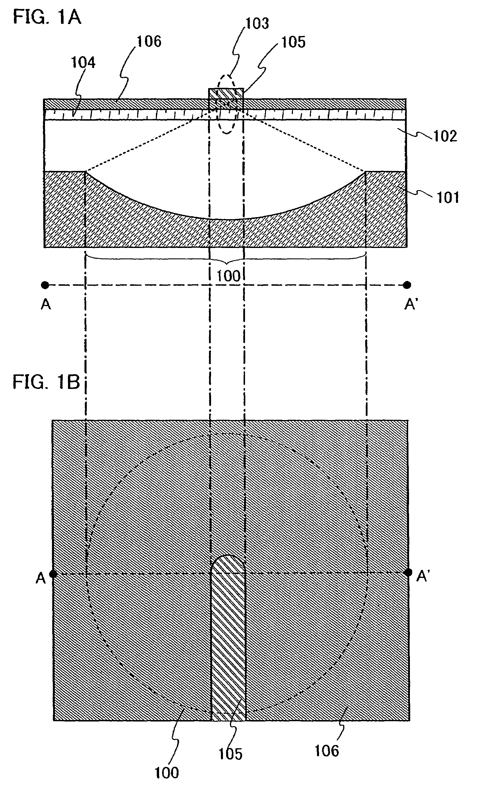
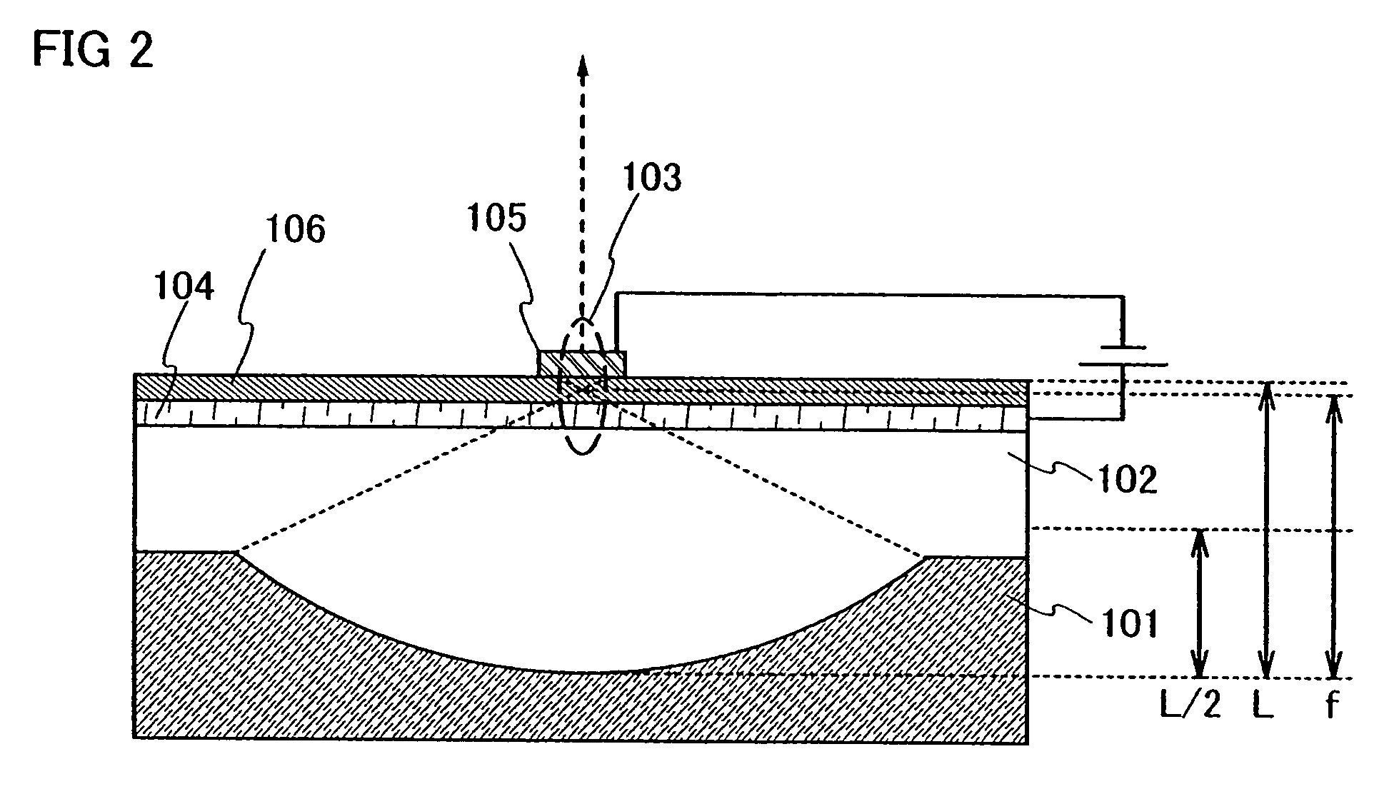
[0089]FIG. 7A is a top view of a laser oscillator according to Example 2 when an anode for a light-emitting element is manufactured. FIG. 7B is a cross-sectional view taken along line A-A′ of FIG. 7A. In a laser oscillator according to Example 2, an anode 604 is formed to overlap with each a plurality of concaves 600 over a first layer 601 that has the plurality of concaves 600. The anode 604 is formed by a material that is reflects light to be served as a reflector.

[0090]In Example 2, the anode 604 is used for a reflector. However, Example 2 is not limited thereto. A reflective film serving as a reflector may be formed over the concave portion, and an anode having light-transmitting properties may be formed over the reflective film.

[0091]FIG. 8A is a top view of a laser oscillator according to Example 2 when a light-emitting element is m...

example 3

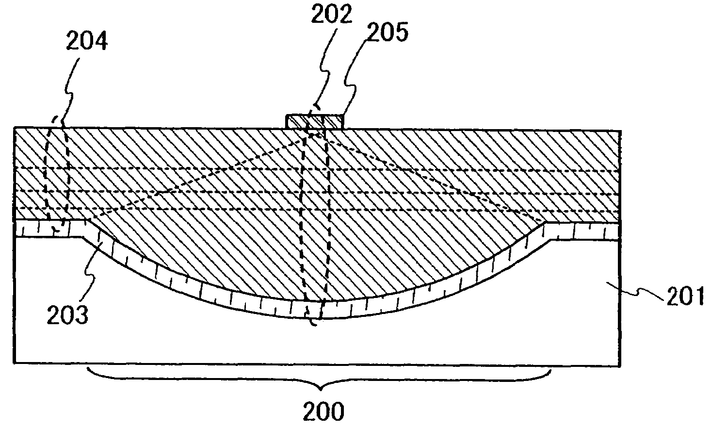
[0096]One mode of a laser oscillator shown in FIG. 9 in which a reflective film capable of reflecting light is formed between a first and a second layers is explained in Example 3.

[0097]FIG. 9 is a cross-sectional view of a laser oscillator according to Example 3. In the laser oscillator according to Example 3 as shown in FIG. 9, a reflective film 802 is formed over a first layer 801 having a concave portion 800. The reflective film 802 can be formed by a material capable of reflecting light by vapor deposition. As the material for the reflective film 802, a material containing one or a plurality of metal elements such as Al, Ag, Ti, W, Pt, or Cr can be used. A material for the reflective film is not limited to the foregoing materials. Any material can be used as long as it can reflect light. For example, the reflective film may be formed by stacking a plurality of insulating film, each of which has different refractive indexes, such as a silicon oxide film, a silicon nitride film, ...


PUM


Abstract

A light-emitting device is disclosed as typified by a laser oscillator formed by an electroluminescent material with improved oscillation efficiency of laser light and even reduced power consumption. The disclosed light-emitting device comprises a light-emitting element including a first electrode having a concave portion, an electroluminescent layer serving as a laser medium formed over the first electrode so as to be overlapped with the concave portion, and a second electrode formed over the electroluminescent layer so as to be overlapped with the concave portion, wherein light generated in the electroluminescent layer is resonated between the first electrode and the second electrode and emitted as laser light from the second electrode, an optical axis of the laser light intersects with the second electrode, the first electrode has a curved surface at the concave portion, and a center of curvature of the curved surface is located at the side of the second electrode above the first electrode.

Description

BACKGROUND OF THE INVENTION[0001]1. Field of the Invention[0002]The present invention relates to a light-emitting device including an electroluminescent material.[0003]2. Related Art[0004]A semiconductor laser has advantages of being extremely manufactured into a small-sized and lightweight laser oscillator compared with another gas laser or solid laser. A semiconductor laser has been put to practical use in various fields as an light source for transmitting and receiving signals by means of an optical interconnection in an optical integrated circuit; for recording on an optical disk, optical memory, or the like; for optical communication with an optical fiber as a light guide. The oscillation wavelength of a semiconductor laser has the wide range of blue to infrared. Most oscillation wavelengths of generally used semiconductor lasers are in an infrared region such as a GaAs laser (wavelength 0.84 μm), an InAs laser (wavelength 3.11 μm), an InSb laser (wavelength 5.2 μm), a GaAlAs (...

Claims


Application Information

Patent Timeline
Patent Type & Authority Patents(United States)
IPC IPC(8): H01L33/00H01L33/20H01S5/02H01S5/022H01S5/026H01S5/042H01S5/10H01S5/183H01S5/36H01S5/42H05B33/10H05B33/12H05B33/20H05B33/22H05B33/26
CPCH01S5/0425H01S5/18388H01S5/36H01S5/423H01L33/20H01S5/02212H01S5/02228H01S5/0267H01S5/1039H01S5/14H01L2224/48472H01L2224/73265H01S5/04253H01S5/04256H01S5/02234
Inventor YAMAZAKI, SHUNPEINOMURA, RYOJISHIMOMURA, AKIHISA
Owner SEMICON ENERGY LAB CO LTD
Why Eureka
Try Eureka