Integrated optic waveguide immunosensor

an optic waveguide and immunosensor technology, applied in the field of solid-state biochemical binding assays, can solve the problems of inability to manufacture silica-on-silica waveguides, the detection limit is not believed to be available in a commercially practical and affordable immunosensor, and the detection limit is not believed to be lowered by thin-film waveguides, etc., to achieve the effect of increasing the reflection density intensity

Inactive Publication Date: 2009-05-26
UNIV OF UTAH RES FOUND
View PDF51 Cites 40 Cited by
  • Summary
  • Abstract
  • Description
  • Claims
  • Application Information

AI Technical Summary

Benefits of technology

[0018]The integrated optic waveguide (“IOW”) of the invention is capable of detecting analyte concentrations in the femtomolar (10−18 M) range. Such sensitivity is well beyond that

Problems solved by technology

At present, such sensitivity is not believed to be available in a commercially practical and affordable immunosensor.
However, the potential lowering of the detection limit by use of thin-film waveguides is achievable only if the waveguide material is nonfluorescent and low-loss.
Furth

Method used


Image

  • Integrated optic waveguide immunosensor
  • Integrated optic waveguide immunosensor
  • Integrated optic waveguide immunosensor

Examples


example 1

SiON Composite Waveguide Fabrication

[0043]Waveguides comprising a 1 μm thick film of Si2O3N on SiO2 have been produced as follows. A heated sample holder containing a 4 inch quartz wafer was placed in a plasma-enhanced chemical vapor deposition (PECVD) reactor. Process gasses flowed from the perimeter of the PECVD vessel, over the sample, and were then pumped out of the vessel through a central port. During deposition, the PECVD reactor was maintained at 300° C. and 1.25 Torr, with 50W of power to a 13.56 MHZ generator. The gas mixture consisted essentially of 27 standard cm3 per minute (sccm) silane (SiH4), 500 sccm nitrogen, 200 sccm ammonia, and 1300 sccm nitrous oxide. The respective inlet partial pressures were approximately 17 mTorr, 308 mTorr, 123 mTorr, and 802 mTorr. Under these conditions, the deposition rate was about 590 Å / minute and a 1 μm film was produced in about 15 minutes. These silicon oxynitride films had an approximate elemental ratio of Si:O:N=2:3:1 and a refra...

example 2

Characterization of SiON Waveguide

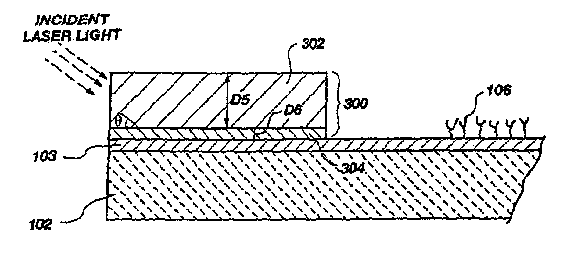
[0046]Scanning electron microscopy was used to examine the shape and thickness of etched channel waveguides. A nominal channel should have optically smooth, rectangular edges and a uniform thickness. For optical characterization of channel waveguides, the beam of the 632.8 nm line from a HeNe laser was coupled into the waveguide using a prism coupler. In a typical experiment, values were determined for waveguide thickness (twg), refractive index (nwg), internal reflection angle (qwg), reflections / cm at the waveguide-superstrate interface (Nr) depth of penetration (dp), and propagation loss (dB / cm). The data of Table 1 summarize the properties measured for a typical SiON waveguide constructed by the procedure outlined

[0047]

TABLE IOptical characterization of SiON waveguideswaveguide parameterair superstratewater superstratetwg (μm)1.31 ± 0.11N.A.nwg1.53 ± 0.0 N.A.propagation loss (dB / cm)0.76 ± 0.09N.D.qwg (degrees)82.67 ± 0.47 82.85 ± 0.42dp (nm)44.10...

example 3

Fabrication of MgF2 / SiO2 Composite Waveguide

[0048]The SiO2 / MgF2 laminates were deposited in situ by electron beam evaporation, using a multipocket electron beam gun in a Balzers BAK760 high-vacuum coater. The deposition chamber was evacuated to 2 μTorr, and the silica chips used as mechanical supports on which the laminates were deposited were heated to 200° C. The chamber pressure rose to 3.8 μTorr as a result of heating of the silica chips prior to deposition. The source materials, 99.9% pure MgF2 and 99.999% pure SiO2, were placed in molybdenum- and graphite-lined hearths, respectively, in the rotatable source carousel. Both source materials were brought to the deposition temperature with the shutter closed. First the MgF2 was evaporated with a slowly sweeping 10-kV (kilovolt) electron beam (≈12 mm2 elliptical spot size) followed by similar evaporation of the SiO2. The deposition rates of MgF2 and SiO2 were controlled at 20 Å / s and 10 Å / s (angstroms per second), respectively, by ...


PUM


Abstract

A composite waveguide for evanescent sensing in fluorescent binding assays comprising a substrate layer having one or more thin-film waveguide channels deposited thereon. Binding molecules having the property of binding with specificity to an analyte are immobilized on the surface of the thin-film channels. In preferred embodiments, the composite waveguide includes integral light input coupling means adapted to the thin-film channels. Light coupling means may include a grating etched into the substrate prior to deposition of the thin film, or a waveguide coupler affixed to the upper surface of the thin film. The waveguide coupler has an input waveguide of high refractive index which receives the laser light through one end, propagating it by total internal reflection. Propagated light is coupled evanescently into the thin film across a spacer layer of precise thickness with a lower index of refraction than that of the input waveguide or the thin-film waveguide.

Description

CROSS REFERENCE TO RELATED APPLICATIONS[0001]This application is a divisional of application Ser. No. 09 / 412,731, filed Oct. 5, 1999 now U.S. Pat. No. 6,350,413, pending, which is a continuation of application Ser. No. 08 / 961,827, filed Oct. 31, 1997, now U.S. Pat. No. 5,961,924, issued Oct. 5, 1999, which is a continuation of application Ser. No. 08 / 393,450, filed on Feb. 23, 1995, now U.S. Pat. No. 5,814,565, issued Sep. 29, 1998.TECHNICAL FIELD[0002]The invention relates to apparatus for solid-state biochemical binding assays, and especially to optical structures utilizing evanescent sensing principles for use in such apparatus and assays.BACKGROUND[0003]Immunoassays exploiting the properties of an optical technique known as total internal reflection (abbreviated “TIR”) are proving to be a valuable tool for detection of analytes at concentrations of 10−10 to 10−13 molar or below, without a wash step. When a light beam traveling in a waveguide is totally internally reflected at th...

Claims


Application Information

Patent Timeline
IPC IPC(8): G01N21/00G01N33/53G01N33/552G02B6/00G01N21/41G01N21/55G01N21/64G01N21/05G01N21/77G01N33/543
CPCG01N21/648G01N21/7703G01N33/54373G01N21/05
Inventor REICHERT, W. MONTYHERRON, JAMES N.CHRISTENSEN, DOUGLAS A.WANG, HSU-KUN
Owner UNIV OF UTAH RES FOUND
Why Eureka
Try Eureka