Highly ionized PVD with moving magnetic field envelope for uniform coverage of feature structure and wafer

a magnetic field envelope and feature structure technology, applied in the field of metalization, can solve the problems of overhang and closure, severe deposition rate and throughput limitations of such a process, and the inability to meet the requirements of the etching system, and achieve the effect of increasing metal ionization

Inactive Publication Date: 2009-07-07
TOKYO ELECTRON LTD
View PDF22 Cites 6 Cited by
  • Summary
  • Abstract
  • Description
  • Claims
  • Application Information

AI Technical Summary

Benefits of technology

[0010]A still further objective of the present invention is to provide an increased metal ionization without additional increasing of the ICP power or DC power at the target.
[0011]Yet another objective of the invention is to provide azimuthally symmetric plasma and flexibility to control and compensate for any azimuthal nonuniformity that could be generated by interaction of the static magnetic field and an ICP source.

Problems solved by technology

), however, at described temperatures the process would result in total agglomeration of Cu seed layers, overhang and closure of via and trenches with large islands of Cu and discontinuous Cu layers.
Reduced temperature requires low power sputtering conditions that would put severe deposition rate and throughput limitations on such a process.
Another limitation would occur when processing wafers in independent deposition and etch systems.
Transferring the wafer between an etch chamber to a separate deposition chamber or between an etch station to a distinct deposition station within the same module has disadvantages both from cost-of-process and quality-of-process points of view.
However, this configuration has a significant disadvantage in that the internal coil is a source of contamination of the film being deposited or etched on the substrate.
Furthermore, the suggestions of Nikei, et al., would result in non-uniform plasma generation and non-uniform etching of the substrate, and in the sequential etching and deposition process, both steps are not uniform across the wafer so as to result in a uniformly processed wafer at the end of the process.

Method used


Image

  • Highly ionized PVD with moving magnetic field envelope for uniform coverage of feature structure and wafer
  • Highly ionized PVD with moving magnetic field envelope for uniform coverage of feature structure and wafer
  • Highly ionized PVD with moving magnetic field envelope for uniform coverage of feature structure and wafer

Examples


Embodiment Construction

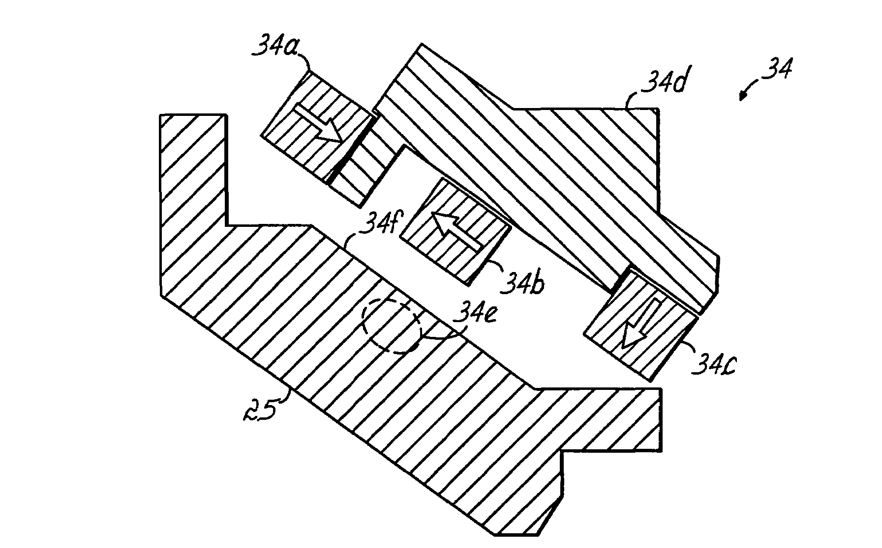
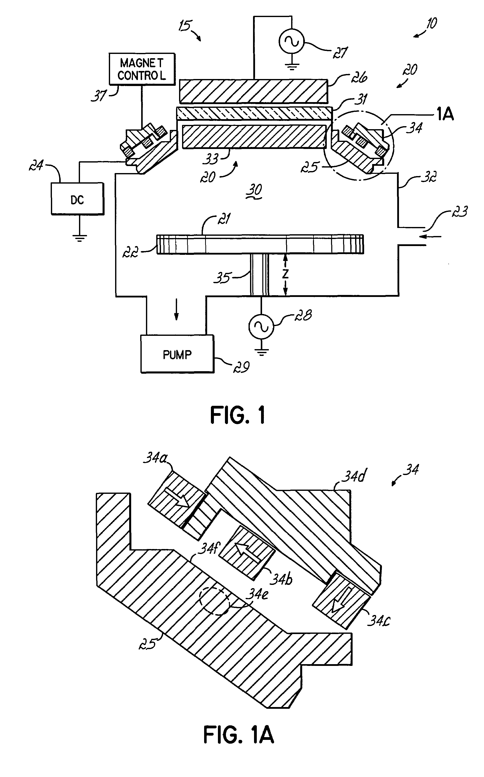
[0035]According to the invention in U.S. Pat. App. Publication No. 20030034244 (Yasar et al.), assigned to the same assignee as current application, a process and an apparatus are provided wherein sequential deposition and etching steps are used to solve problems set forth above. Application of that process may involve first depositing a thin layer of metallization, for example such as tantalum (Ta), tantalum nitride (TaN) or copper (Cu), and then, preferably after stopping the deposition, performing an ion etch step, preferably by ionized gas, for example such as argon (Ar). The etching step removes less material on both the field area on the top surface of the wafer and the via bottom than is deposited during the deposition step, and thus there is net deposition at the end of the process cycle. The deposition-etch cycle can be repeated as many times as needed to achieve a desired result. By balancing the deposition and etching times, rates and other deposition and etch parameters,...


PUM

PropertyMeasurementUnit
pressureaaaaaaaaaa
pressureaaaaaaaaaa
pressuresaaaaaaaaaa

Abstract

This invention relates to ionized PVD processing of semiconductor wafers and provides conditions for highly uniform deposition-etch process sequence and coverage capabilities of high aspect ratio (HAR) features within a single processing chamber. A plasma is generated and maintained by an inductively coupled plasma (ICP) source. A deposition process step is performed in which metal vapor is produced from a target of a PVD source. Location and sputter efficiency at the target surface is enhanced by moving a magnet pack to create a traveling or sweeping magnetic field envelope. The target is energized from a DC power supply and pressures effective for an efficient thermalization of the sputtered atoms (30<p<100 mTorr) are maintained in the chamber during deposition. A uniform thickness of the metal on the wafer is produced within each magnet sweeping cycle. Magnetic field localization using an annular sweeping motion over the entire target surface generates conditions for reasonable deposition rates, high target utilization, high ionization of the metal atoms, uniform flat field deposition and etching, and nearly identical conditions for HAR feature coverage at the center and edge of the wafer.

Description

[0001]This application is related to U.S. patent application Ser. No. 10 / 795,093, filed Mar. 5, 2004, which is a continuation-in-part of U.S. patent application Ser. No. 10 / 138,049 filed May 3, 2002, which claims priority to U.S. Provisional Patent Application Ser. No. 60 / 288,952, filed May 4, 2001, each hereby expressly incorporated herein by reference.FIELD OF THE INVENTION[0002]This invention relates to the metallization of via and trench structures on semiconductor wafers. More particularly, the invention relates to the metallization of high aspect ratio via and trench structures of silicon wafers utilizing ionized sputtered materials to form barrier and seed layers.BACKGROUND OF THE INVENTION[0003]Ionized PVD has been utilized in semiconductor processing for metallization and interconnects, and appears promising for extension to submicron technology. In the metallization of high aspect ratio (HAR) via holes and trenches on semiconductor wafers, it has been considered important ...

Claims


Application Information

Patent Timeline
Patent Type & Authority Patents(United States)
IPC IPC(8): C23C14/00C25B11/00C25B13/00C23C14/04C23C14/35H01J37/34
CPCC23C14/046C23C14/3492C23C14/358H01J37/3405H01J37/3455H01J37/321H01J2237/3327A61P31/04
Inventor BRCKA, JOZEF
Owner TOKYO ELECTRON LTD
Why Eureka
Try Eureka