Group III nitride compound semiconductor light emitting device

a light emitting device and nitride technology, applied in the direction of semiconductor devices, electrical devices, nanotechnology, etc., can solve the problems of lattice mismatching and light emission efficiency reduction, and achieve the effects of suppressing the diffusion of p-type impurities, enhancing the efficiency of hole injection from the p-type semiconductor layer to the active layer, and improving the light emission efficiency of the light emitting devi

Active Publication Date: 2009-08-18
TOYODA GOSEI CO LTD
View PDF8 Cites 28 Cited by
  • Summary
  • Abstract
  • Description
  • Claims
  • Application Information

AI Technical Summary

Benefits of technology

[0017]Consequently, a hole injection efficiency from the p-type semiconductor layer to the active layer can be enhanced. Accordingly, the light emission efficiency of the light emitting device can be improved.
[0018]When a barrier layer which is the closest to the p-type semiconductor layer is set to be a thin film, generally, the p-type impurity of the p-type semiconductor layer is easily diffused into the active layer, which is not preferable. According to the invention, however, the doping amount of the p-type impurity in the first layer which is

Problems solved by technology

When the p-type impurity is diffused into the active layer, the quality of the crystal of the active layer is deteriorated, causing a reduction i

Method used


Image

  • Group III nitride compound semiconductor light emitting device
  • Group III nitride compound semiconductor light emitting device
  • Group III nitride compound semiconductor light emitting device

Examples


example)

[0052](Example)

[0053]An example of the invention will be described below.

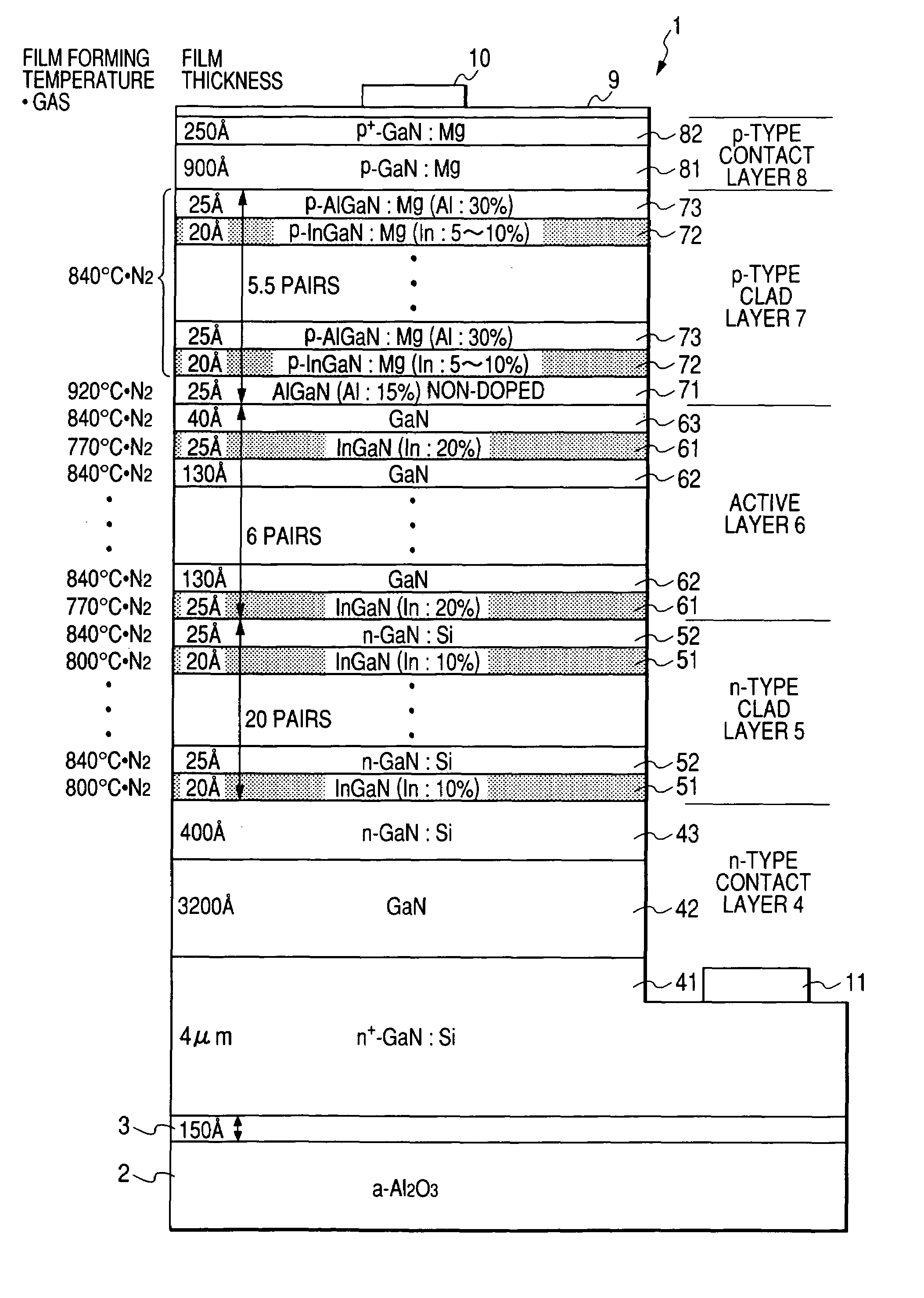
[0054]The example relates to a light emitting diode 1 and a structure thereof is shown in FIG. 1.

[0055]Sapphire is employed for a substrate 2 and a group III nitride compound semiconductor layer is laminated on an “a” surface thereof. It is possible to use, as a substrate material, a hexagonal material such as SiC (silicon carbide) and GaN (gallium nitride) and a cubic material such as Si (silicon), GaP (gallium phosphide) and GaAs (gallium arsenide) in addition to the sapphire.

[0056]An AlN buffer layer 3 is formed on the sapphire substrate 2 by sputtering. The buffer layer 3 can also be formed by another method such as an MOCVD method. Moreover, it is also possible to form a buffer layer by another group III nitride compound semiconductor material such as GaN in addition to AlN.

[0057]The group III nitride compound semiconductor layer shown in FIG. 1 is formed on the buffer layer 3 by a related method (MOCVD me...


PUM


Abstract

In a group III nitride compound semiconductor light emitting device comprising an n-type semiconductor layer, a p-type semiconductor layer having a superlattice structure in which a first layer comprising at least Al and a second layer having a different composition from that of the first layer are laminated repetitively, and an active layer interposed between the n-type semiconductor layer and the p-type semiconductor layer, wherein an Al composition of the first layer which is the closest to the active layer is set to be lower than that of each of the other first layers, and wherein a doping amount of a p-type impurity in the first layer which is the closest to the active layer is set to be smaller than that of the p-type impurity of each of the other first layers or non-doped.

Description

[0001]This application is based on Japanese Patent Application No. 2004-296706, which is incorporated herein by reference.BACKGROUND OF THE INVENTION[0002]1. Field of the Invention[0003]The present invention relates to a group III nitride compound semiconductor light emitting device.[0004]2. Description of the Related Art[0005]A group III nitride compound semiconductor light emitting device has such a structure that an active layer is interposed between an n-type semiconductor layer and a p-type semiconductor layer. In order to increase a light emission efficiency in the light emitting device, the active layer is set to have a multiple quantum well structure in some cases. Also in the n-type semiconductor layer and the p-type semiconductor layer, a superlattice structure is employed in some cases. By employing the superlattice structure in the n-type semiconductor layer and the p-type semiconductor layer, the resistance of each layer is reduced so that an electron injection efficien...

Claims


Application Information

Patent Timeline
IPC IPC(8): H01L33/00H01L33/06H01L33/32
CPCB82Y20/00H01L33/32H01L33/06H01L33/025
Inventor UEMURA, TOSHIYASAWAZAKI, KATSUHISANAKAI, MASAHITOIKEMOTO, YUHEI
Owner TOYODA GOSEI CO LTD
Why Eureka
Try Eureka