
Layered ceramic capacitor

a ceramic capacitor and layered technology, applied in the direction of fixed capacitors, stacked capacitors, fixed capacitor details, etc., can solve the problems of reduced effective area, high cost of noble metal, and reduced use of noble metal in terms of cost, so as to achieve large capacitance and high reliability

Active Publication Date: 2009-09-29
TDK CORPARATION
View PDF6 Cites 14 Cited by
  • Summary
  • Abstract
  • Description
  • Claims
  • Application Information

AI Technical Summary

Benefits of technology

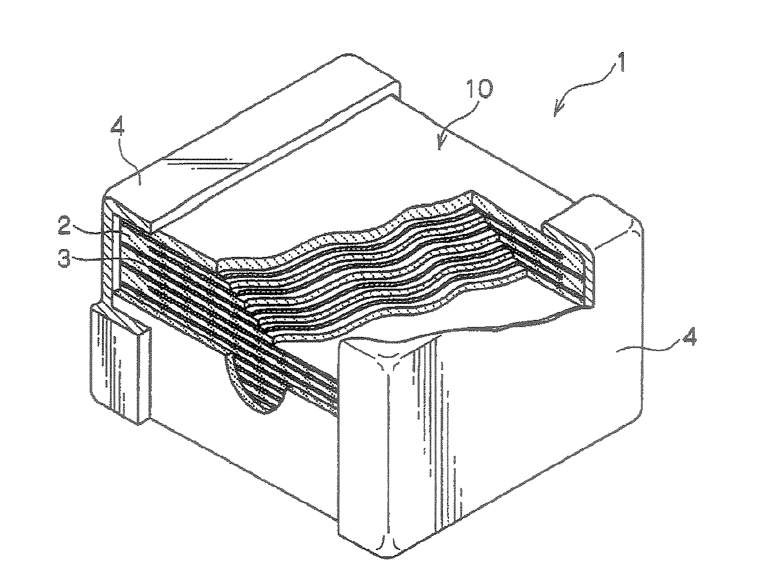
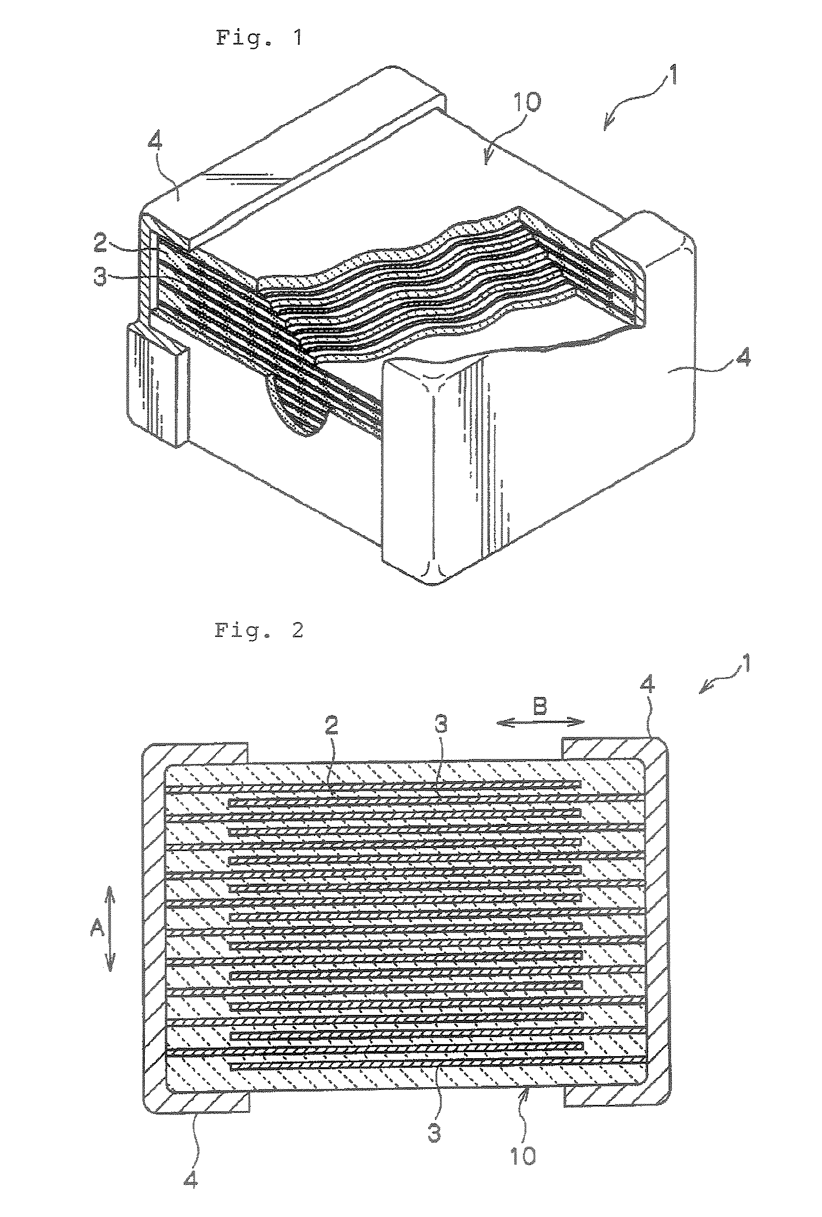
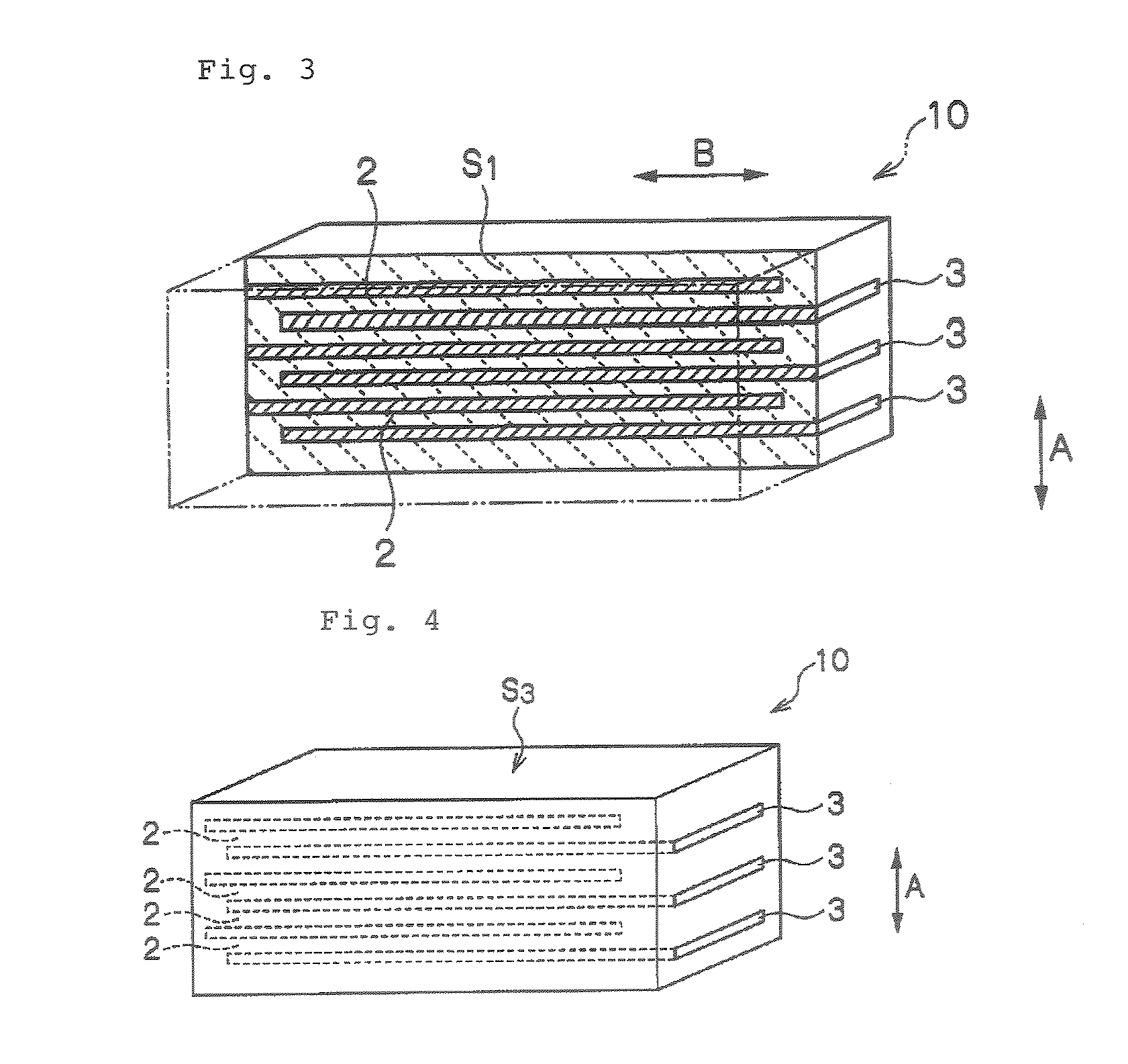
[0010]The present invention was conceived in consideration of the circumstances encountered in making thin the dielectric layer and increasing the layered number of the dielectric layers with the miniaturization of the multilayer ceramic capacitor. An object of the present invention is to provide a multilayer ceramic capacitor having a large capacitance and a high reliability.
[0020]According to this fourth aspect, since the equations LS=−Ln(n)×B and 10≦B≦300 are satisfied in the described conditions, as a result, the multilayer ceramic capacitor obtained by using such layered dielectric body can provide a high dielectric constant and a large capacitance.
[0022]According to such embodiment, the sintering temperature at the time of forming the internal electrode layers is lowered, and hence, the temperature difference from the sintering temperature of the dielectric layers can be made large as well as the difference in contraction coefficient. As a result, a further large residual stress can be provided to the multilayer ceramic capacitor of the above aspects, which can provide a high dielectric constant and a large capacitance.
[0023]In the other preferred embodiment, the dielectric layer between two internal electrode layers has a thickness of not more than 5 μm and more preferably of not more than 2 μm. According to this embodiment, the thickness of the dielectric layer has small difference in thickness from that of the internal electrode layer. Accordingly, the effect due to the difference in the sintering behavior between the dielectrics and the internal electrode material (Ni or Ni alloy) can be remarkably attained, so that the large residual stress can be obtained, and as a result, the multilayer ceramic capacitor having a high dielectric constant can be obtained.
[0027]As mentioned above, according to the multilayer ceramic capacitor of the present invention of the characteristics mentioned above, as the residual stress becomes large, the dielectric constant also large. Thus, the multilayer ceramic capacitor having a large residual stress can provide a large capacitance and, hence, the multilayer ceramic capacitor can be miniaturized. Furthermore, according to the present invention, by utilizing the difference in the sintering behaviors between the dielectric layer and the internal electrode layer, a large residual stress can be provided to the multilayer ceramic capacitor, and as a result, a high dielectric constant and a large capacitance can be realized, thus being advantageous.

Problems solved by technology

However, such noble metal is expensive and the use thereof is hence not reasonable in terms of cost.
However, the small-sized structure of the multilayer ceramic capacitor will result in a reduction of effective area.
However, a structural defect may easily occur by making thinning of the dielectric layer, and increasing the number of the laminated dielectric layers.
This problem becomes prominent with increasing the number of the laminated dielectric layers, and much severe in recent technology in which the thickness of the dielectric layer becomes thinner and the number of the laminated dielectric layers becomes increased to satisfy the requirement of the small-sized structure and large capacitance thereof.

Method used


Image

  • Layered ceramic capacitor
  • Layered ceramic capacitor
  • Layered ceramic capacitor

Examples


first experiment 1

[0129

[0130]Pastes for the dielectric layers, the internal electrode layers and the external electrodes were firstly prepared as follows.

[0131]Paste for Dielectric Layers

[0132](MgCO3)4.Mg(OH)2.5H2O, MnCO3, BaCO3, CaCO3, SiO2, Y2O3, and V2O5 were added to Ba1.005TiO3 manufactured by the hydrothermal synthesis method, which are then wet-blended by a ball mill for 16 hours to thereby obtain a dielectric material containing, as final composition, Ba1.005 TiO3 of 100 mol %, MgO of 2 mol %, MnO of 0.4 mol %, Y2O3 of 2 mol %, V2O5 of 0.01 mol %, and Ba,Ca)SiO3 of 3 mol %. Then, the dielectric material of 100 unit weights, acrylate resin of 4.8 unit weights, methylene chloride of 40 unit weights, trichloroethane of 20 unit weights, mineral spirit of 6 unit weights, and acetone of 4 unit weights were mixed and kneaded in the ball mill to obtain a paste for the dielectric layers.

[0133]Paste for Internal Electrode Layers

[0134]Ni powder of average particle size of 0.4 μm of 100 unit weights, org...


PUM

PropertyMeasurementUnit
particle sizeaaaaaaaaaa
thicknessaaaaaaaaaa

Abstract

A multilayer ceramic capacitor having a high dielectric constant, a large capacitance and a high reliability can be obtained by controlling a value of residual stress in it.

Description

FIELD OF THE INVENTION[0001]The present invention relates to a multiplayer (layered) ceramic capacitor, and more particularly, to a small-sized (i.e., miniaturized) multilayer ceramic capacitor having thin dielectric layers capable of achieving a high dielectric constant and a large capacitance.BACKGROUND ART[0002]A multilayer ceramic capacitor has been widely utilized as an electric parts having small size and large capacitance with high reliability, and a plurality of such multilayer ceramic capacitors have been arranged in an electronic equipment[0003]In recent years, there it has been required for the electronic equipment to provide a small-sized and a high reliability, and such requirement has also been desired for the multilayer ceramic capacitor so as to realize a down-sizing, a large capacitance, a low price and a high reliability.[0004]The multilayer ceramic capacitor includes a layered dielectric body which is formed by alternately laminating dielectric layers and internal...

Claims


Application Information

Patent Timeline
Patent Type & Authority Patents(United States)
IPC IPC(8): H01G4/06H01G4/008H01G4/12H01G4/30
CPCH01G4/30H01G4/1227H01G4/12
Inventor NAKANO, YUKIENOMURA, TAKESHITAGUCHI, YASUTAKA
Owner TDK CORPARATION
Learn More