Near-field optical head having tapered hole for guiding light beam

a technology of optical head and guiding light beam, which is applied in the field of near-field optical head, can solve the problems of difficult to read and write signals, difficult to maintain a distance between the disk and the aperture, and the head is difficult to control the position relative to the disk motion, etc., and achieves the effect of increasing the speed of rotation of the recording medium and high speed

Inactive Publication Date: 2009-10-06
SEIKO INSTR INC
View PDF43 Cites 61 Cited by
  • Summary
  • Abstract
  • Description
  • Claims
  • Application Information

AI Technical Summary

Benefits of technology

[0019]Accordingly, once reflection of light upon the light reflection layer makes it possible to focus the light to a vicinity of the very small aperture. This can increase the intensity of near field light produced from the aperture and provide a near field optical head high in mechanical strength, compact in structure and excellent in mass producibility.
[0140]Accordingly, by two-dimensionally scanning the near field optical head and simultaneously processing a plurality of ones of microscopic bit information at a plurality of very small apertures, it is possible to implement processing entirely at high speed without the necessity of increasing the speed of rotation of the recording medium.

Problems solved by technology

Thus, the head is difficult to control in position relative to disk motion.
Further, the head structured in large size makes it impossible to maintain a distance between the disk and the aperture.
This results in a situation that the output SN ratio from optical information depicted on the disk is lowered thus making it difficult to read and write signals.
Meanwhile, the greater part of light attenuates before reaching the aperture thus making it difficult to produce sufficient near-field light from the aperture for implementing reading-out at high speed.
Furthermore, the structure having the upwardly extending fibers increases the size of apparatus itself making difficult to reduce the size and thickness thereof.
There is a necessity of separately providing a structure that moves responsive to movement of the head thus encountering difficulty.
Also, the separate provision of such a structure increases the size of the apparatus itself and the size reduction of the reading-out and recording apparatus is difficult.
Furthermore, where keeping constant a distance to a media through the interaction with a media surface by use of an optical fiber probe having optical fiber sharpened at its tip or a cantilever-type optical probe sharpened at its tip, scanning should be made while controlling a distance to the media at all times. This requires a feedback apparatus therefor and making difficult to reduce the size of the recording and reading-out apparatus.
Furthermore, there is also a problem in high speed scanning because of a limitation of response speed of the feedback system.
Also, the tip-sharpened probe is not sufficient in mechanical strength and hence not suited for being arrayed.
Also, the intensity of near-field light from the aperture is not sufficient due to light loss at a fiber tip.
Also, the probe is manually fabricated one by one and lack in mass producibility.
Meanwhile, the planar probe requires light to be incident from above thus posing a problem with apparatus size increase and mass producibility or a problem with reduction in flexture function as encountered in the above problem.
Furthermore, the probe aperture must be formed in a size smaller than a wavelength of propagation light (laser light, etc.) in order to produce near-field light or scatter near-field light. it is however difficult to fabricate such a size (10 nano-meters to 200 nano-meters) of an aperture to an objective shape and size with accuracy and reproducibility.
There are cases of encountering problems concerning silicon substrate quality or etch solution concentration nonuniformity.
This results in unetching in a direction or at a rate as intended in areas containing crystalline defects or impurities, causing errors in the shape or size of a finally available aperture.
Meanwhile, the problem with etch solution concentration nonuniformity in the latter case means that there is more or less nonuniformity of concentration in an etch solution and such concentration nonuniformity causes an area that etching advances at a high rate and that advances at a low rate on a silicon substrate, i.e. there appear areas different in etch rate resulting in causing errors in the shape or size of a finally obtained aperture.
Such a problem cannot be neglected particularly for a case where a multiplicity of planar probes are to be formed on a silicon wafer, thus posing a cause of incurring reduction of yield.

Method used


Image

  • Near-field optical head having tapered hole for guiding light beam
  • Near-field optical head having tapered hole for guiding light beam
  • Near-field optical head having tapered hole for guiding light beam

Examples


embodiment 1

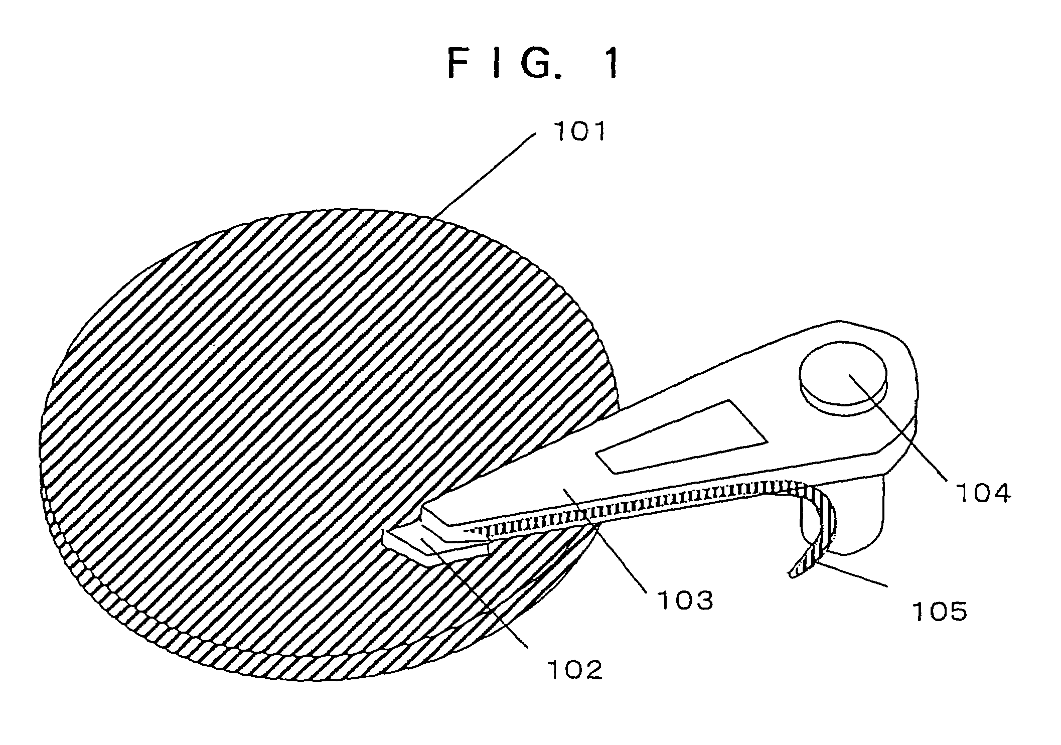
[0188]FIG. 1 illustrates a schematic view of an example of an optical storing and reading-out apparatus according to Embodiment 1 of the invention. A near-field optical head 102 is arranged over a disk 101 (media) rotating at high speed to keep a constant distance to the disk 101 due to a floating force undergone by fluid motion caused by the rotation and a load weight of an arm 103. The way of keeping the distance to the disk 101 may adopt a method to control the interaction, such as tunnel current or interatomic force, caused between the near-field optical head 102 and the media surface. The near-field optical head 102 is supported at a tip of the arm 103. By moving the arm 103 in a horizontal direction by a rotary shaft 104 having a motor, the near-field optical head 102 can be scanned to an arbitrary point on the disk 101. The light propagated through an optical waveguide (or may be an optical fiber) 105 connected to the arm 103 is introduced into an optical waveguide (light int...

embodiment 2

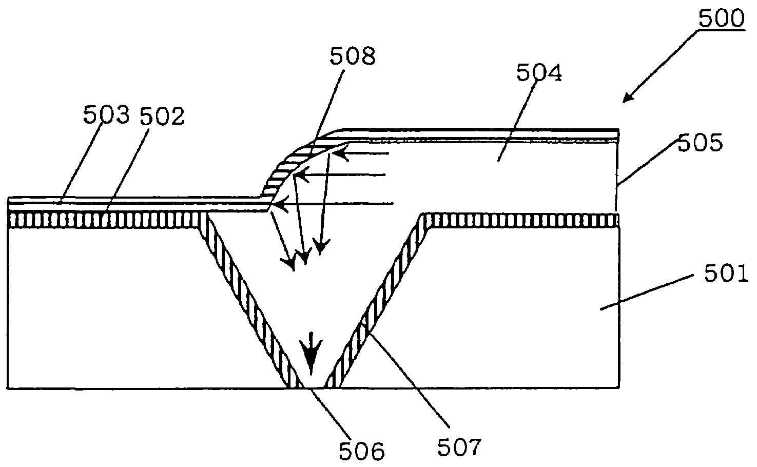
[0209]FIG. 8 shows a sectional view of a part of a near-field optical head 800 according to Embodiment 2. In FIG. 8, an optical waveguide 804 is provided through a light reflection film 802 on a silicon substrate 801 having an aperture 806 and further a light reflection film 803 is provided thereon, similarly to the near-field optical head 500 according to Embodiment 1. The aperture 806 has a microscopic diameter of less than 200 nano-meters in order to produce near-field light due to light introduced through a taper 807.

[0210]The near-field optical head 800 according to Embodiment 2 is in a structure possessing a focusing function in the optical waveguide layer 804 to cause light to be incident on a light incident end 805 for light incidence. If as shown in FIG. 8 the light incident end 805 is made in shape in a convex surface form, the light emitted from a laser light source or optical fiber not shown in the figure is incident at the light incident end 805 into the optical wavegui...

embodiment 3

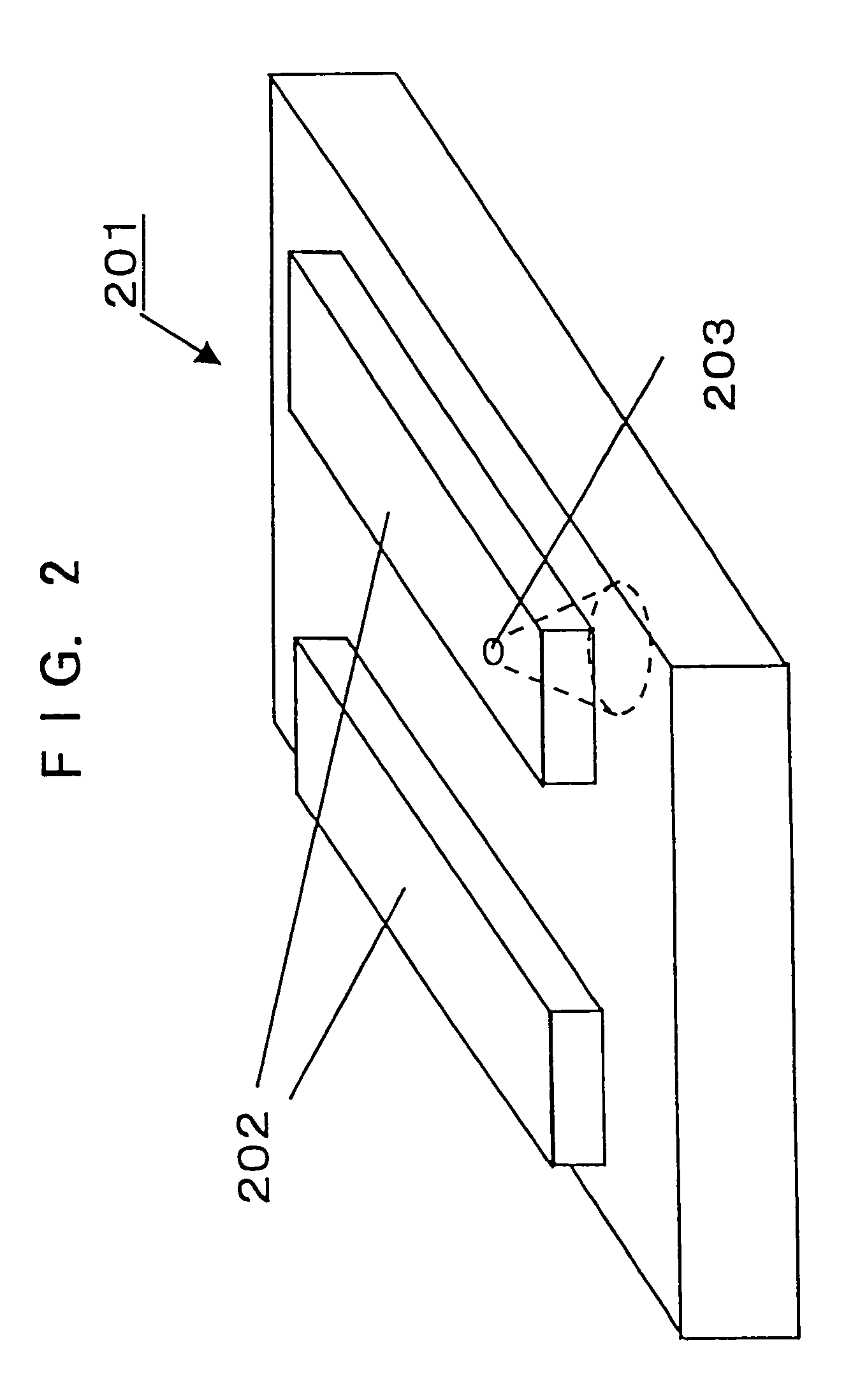
[0215]FIG. 9 shows a sectional view of part of a silicon substrate constituting for a near-field optical head according to Embodiment 3. In FIG. 9, a silicon substrate is illustrated wherein a taper is formed by two different slant surfaces.

[0216]The near-field optical head of Embodiment 3 is improved in optical efficiency in the vicinity of an aperture by making moderate the slant surface in the vicinity of the aperture, i.e. widening the taper angle in the vicinity of the aperture. For propagation light in general, propagation loss is greater in a region where the optical waveguide for light propagation is smaller in width than a wavelength λ. Accordingly, by widening the angle of the taper in the vicinity of the aperture, the region that the width is smaller than the wavelength λ is decreased thus making possible to increase the amount of light reaching the aperture. This results in increase in intensity of near-field light to be caused through the aperture.

[0217]The taper 507 in...


PUM

PropertyMeasurementUnit
slant angleaaaaaaaaaa
angleaaaaaaaaaa

Abstract

A near-field optical head has a planar substrate having a first surface, a second surface disposed opposite to the first surface, and an inverted conical or pyramidal hole extending through the first and second surfaces. The conical or pyramidal hole has at least one fine aperture formed at an apex thereof and is disposed on the first surface of the planar substrate. An optical waveguide is disposed on the second surface of the planar substrate for propagating light. A light reflection film is disposed in the optical waveguide for reflecting in the direction of the fine aperture light propagated through the optical waveguide.

Description

CROSS-REFERENCE TO RELATED APPLICATIONS[0001]This application is a U.S. national stage application of copending International Application Ser. No. PCT / JP99 / 06150, filed Nov. 4, 1999, claiming a priority date of Nov. 9, 1998, and published in a non-English language.TECHNICAL FIELD[0002]The present invention relates to a near-field optical head for an information recording and reading-out apparatus which can record and read-out information with high density by reading-out structural or optical information formed in very small area and recording information to very small area by utilization of near-field light caused by optical interaction in the very small area.BACKGROUND OF THE INVENTION[0003]The information recording and reading-out apparatuses using light is advancing toward increase of capacity and decrease of size, requiring recording bit density increase. As a countermeasure there are studies using violet semiconductor lasers or SIL (Solid Immersion Lens). With these technologie...

Claims


Application Information

Patent Timeline
Patent Type & Authority Patents(United States)
IPC IPC(8): G11B7/00G01Q60/18G01Q60/22G01Q80/00G02B6/12G02B6/42G02B21/00G02B27/56G11B5/02G11B7/12G11B7/135G11B7/22
CPCG11B7/1203G11B7/125G11B7/1362G11B7/1387G11B7/22G11B7/124B82Y10/00B82Y20/00G01Q80/00G02B6/4214G11B2007/13727G11B7/122
Inventor KATO, KENJINIWA, TAKASHIICHIHARA, SUSUMUCHIBA, NORIOOUMI, MANABUKASAMA, NOBUYUKIMITSUOKA, YASUYUKI
Owner SEIKO INSTR INC
Why Eureka
Try Eureka