Semiconductor device having a sense amplifier array with adjacent ECC

a technology of semiconductor memory and amplifier array, which is applied in the direction of digital storage, instruments, coding, etc., can solve the problems of significant increase of devices, degraded dram operating margin, and reduced voltage, so as to reduce the penalty of operation speed due to delay time of wiring, the effect of increasing the integration density

Active Publication Date: 2009-10-13
MICRON TECH INC
View PDF9 Cites 43 Cited by
  • Summary
  • Abstract
  • Description
  • Claims
  • Application Information

AI Technical Summary

Benefits of technology

[0008]In particular, the mismatch in threshold voltage of MOS transistors which form the sense amplifier and the reduction in the voltage at the storage node due to the junction leakage current cause serious problems. Further scaling leads to the increase of mismatch in threshold voltage because the number of impurities in the channel of the miniaturized MOS transistor significantly fluctuates. Further, the junction leakage current is also increased because the electric field in the diffusion layer becomes stronger due to the miniaturization. Due to the device variations as described above, the effective amplitude of signals at the time when the data is read from the memory cell is reduced, and the risk that the data is erroneously read out when the signals are amplified by the sense amplifier is increased.
[0021]The effects obtained by typical aspects of the present invention will be briefly described below. That is, it is possible to efficiently reduce the area penalty and the operation cycle penalty caused by providing an error correction code circuit in a semiconductor memory device.

Problems solved by technology

However, when the memory cell transistors are miniaturized, the variation in devices is significantly increased, and the operating margin of the DRAM is degraded due to the variation and the influence of the voltage reduction in combination.
In particular, the mismatch in threshold voltage of MOS transistors which form the sense amplifier and the reduction in the voltage at the storage node due to the junction leakage current cause serious problems.
Further scaling leads to the increase of mismatch in threshold voltage because the number of impurities in the channel of the miniaturized MOS transistor significantly fluctuates.
Further, the junction leakage current is also increased because the electric field in the diffusion layer becomes stronger due to the miniaturization.
Due to the device variations as described above, the effective amplitude of signals at the time when the data is read from the memory cell is reduced, and the risk that the data is erroneously read out when the signals are amplified by the sense amplifier is increased.
The DRAM chip with such a large area penalty is difficult to apply to cost-conscious products such as a server, a personal computer (PC) and electric appliances.

Method used


Image

  • Semiconductor device having a sense amplifier array with adjacent ECC
  • Semiconductor device having a sense amplifier array with adjacent ECC
  • Semiconductor device having a sense amplifier array with adjacent ECC

Examples


Embodiment Construction

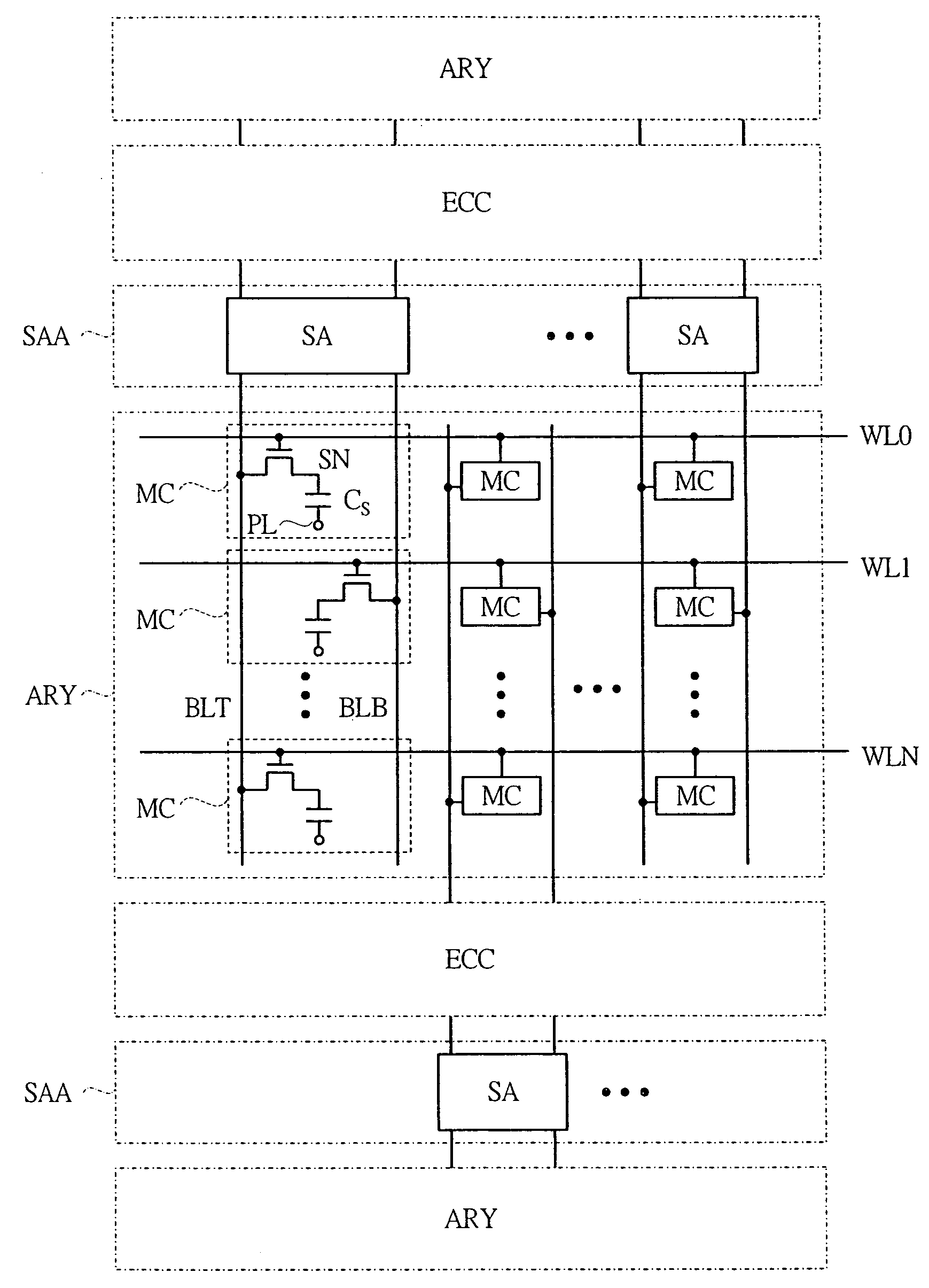
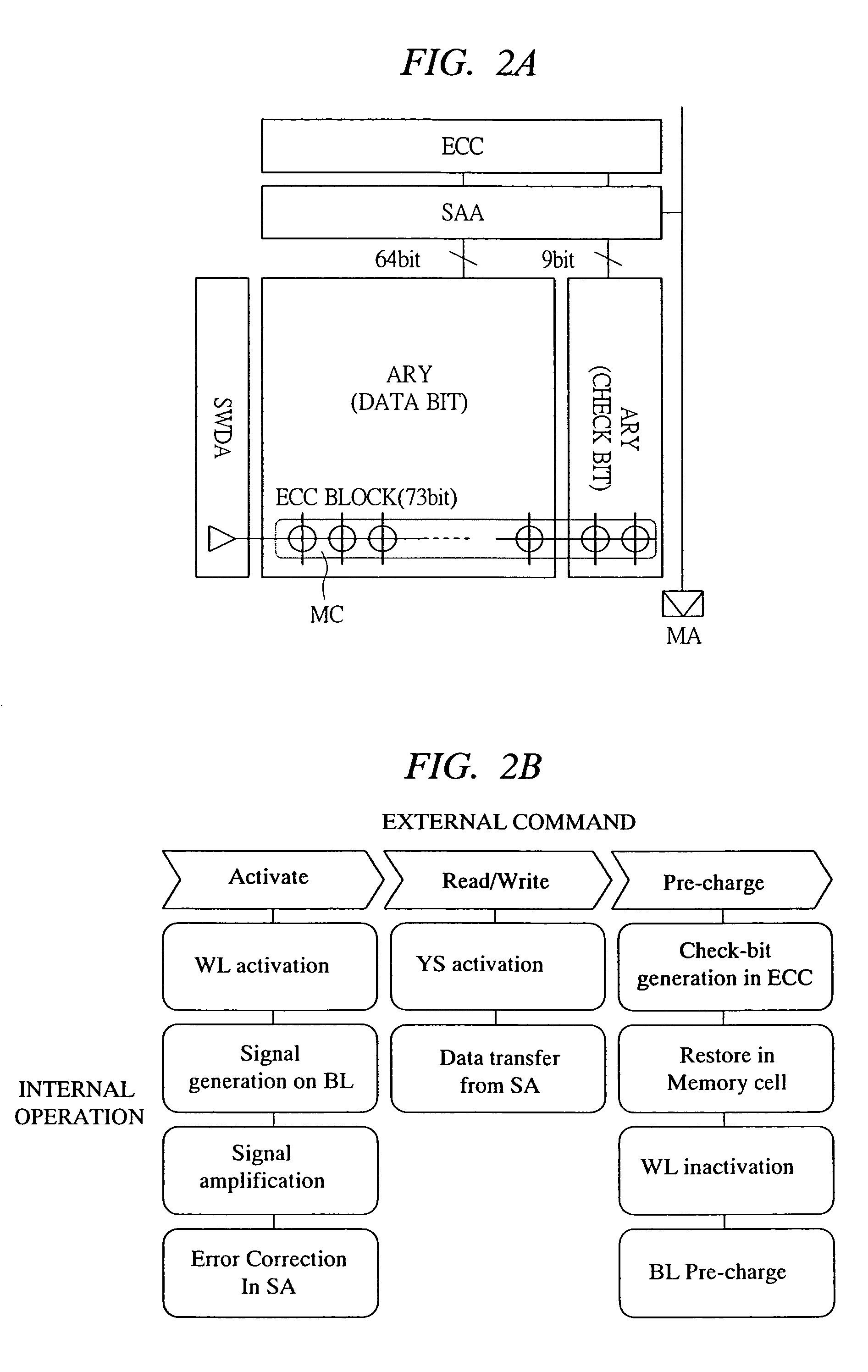
[0048]Hereinafter, embodiments of the present invention will be described in detail with reference to the accompanying drawings. Note that components having the same function are denoted by the same reference symbols throughout the drawings for describing the embodiment, and the repetitive description thereof will be omitted. Also, in the drawings, an arrow mark is attached to a gate of the PMOS transistor so as to distinguish it from the NMOS transistor. Furthermore, though the connection of the substrate potential of the MOS transistors is not particularly described in the drawings, any connection method can be employed as long as MOS transistors can be normally operated.

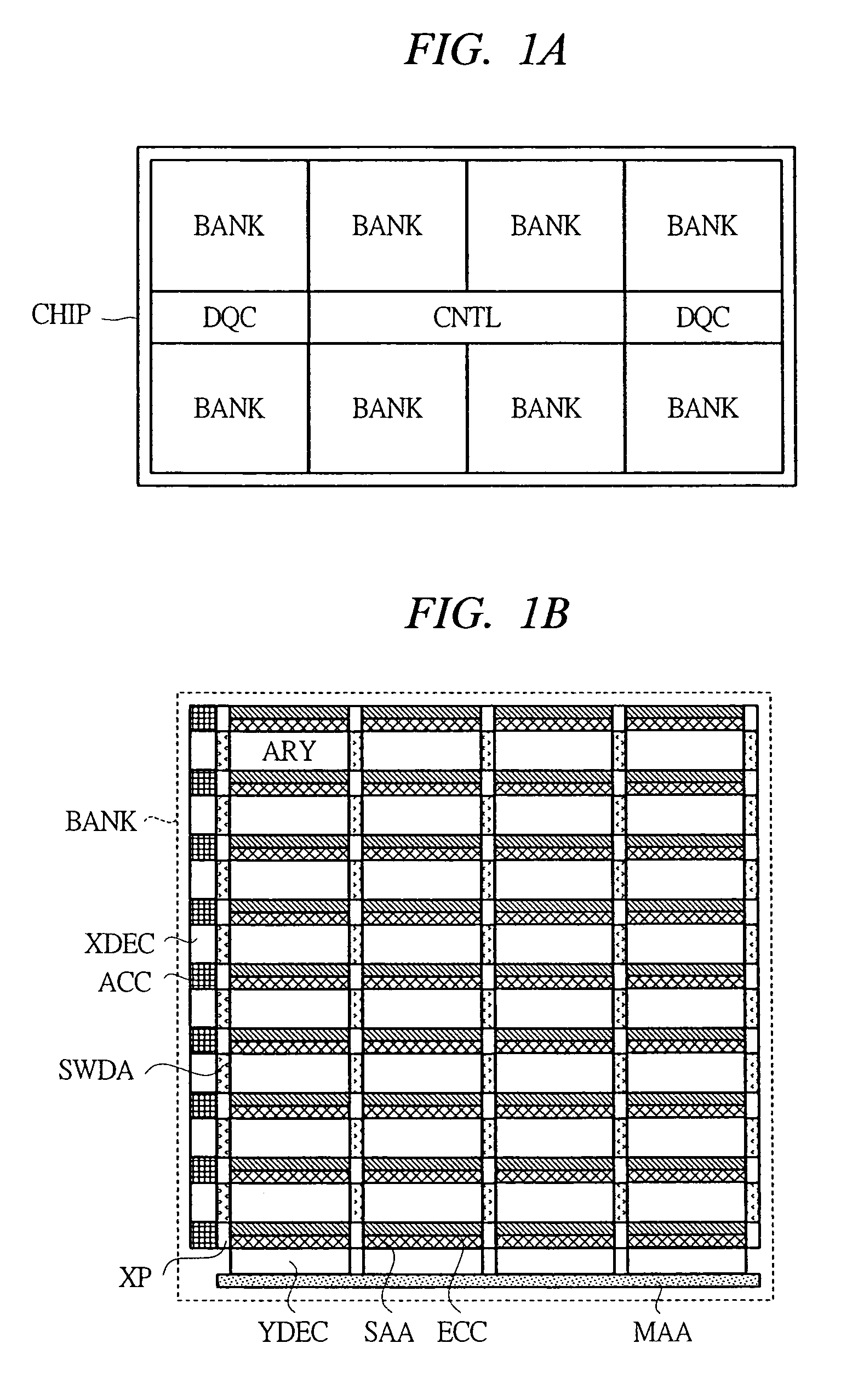
[0049]FIG. 1 is a plan view showing an example of a chip structure in a semiconductor memory device according to an embodiment of the present invention, in which FIG. 1A shows an example of the structure of the entire chip, and FIG. 1B shows an example of the structure of a memory bank in FIG. 1A.

[0050]The semicon...


PUM


Abstract

A semiconductor memory device capable of achieving a sufficient operating margin without increasing an area penalty even in the case of miniaturization is provided. An error correction system composed of a data bit of 64 bits and a check bit of 9 bits is introduced to a memory array such as DRAM, and an error correction code circuit required therein is disposed near a sense amplifier array. In addition to normal memory arrays composed of such memory arrays, a redundant memory array having a sense amplifier array and an error correction code circuit adjacent thereto is provided in a chip. By this means, the error which occurs in the manufacture can be replaced. Also, the error correction code circuit corrects the error at the time of an activate command and stores the check bit at the time of a pre-charge command.

Description

CROSS-REFERENCE TO RELATED APPLICATION[0001]The present application claims priority from Japanese Patent Application No. JP 2005-223012 filed on Aug. 1, 2005, the content of which is hereby incorporated by reference into this application.TECHNICAL FIELD OF THE INVENTION[0002]The present invention relates to a semiconductor memory device. More particularly, it relates to a semiconductor memory such as a dynamic random access memory (DRAM) mounted with an error correction code circuit.BACKGROUND OF THE INVENTION[0003]According to the study by the inventors of the present invention, the following technologies for improving the reliability of the DRAM are known.[0004]For example, Japanese Patent Application Laid-Open Publication No. 2003-77294 (Patent Document 1) describes a memory circuit as shown in FIG. 21. The memory circuit shown in FIG. 21 has a structure in which the data from memory cells of SRAM or DRAM is checked and corrected in the error correction code circuits (ECC circuit...

Claims


Application Information

Patent Timeline
Patent Type & Authority Patents(United States)
IPC IPC(8): G11C29/00
CPCG06F11/1044G11C2029/0409
Inventor SEKIGUCHI, TOMONORITAKEMURA, RIICHIROAKIYAMA, SATORUHANZAWA, SATORUKAJIGAYA, KAZUHIKO
Owner MICRON TECH INC
Why Eureka
Try Eureka