Methods of making spintronic devices with constrained spintronic dopant

a spintronic and dopant technology, applied in the field of spin-based electronics, can solve the problems of low thermal stability, limited current spintronics technology, and low use efficiency, and achieve the effect of reducing the probability of precipitation of spintronic dopant and high spintronic dopant concentration

Active Publication Date: 2009-12-01
ATOMERA INC
View PDF11 Cites 90 Cited by
  • Summary
  • Abstract
  • Description
  • Claims
  • Application Information

AI Technical Summary

Benefits of technology

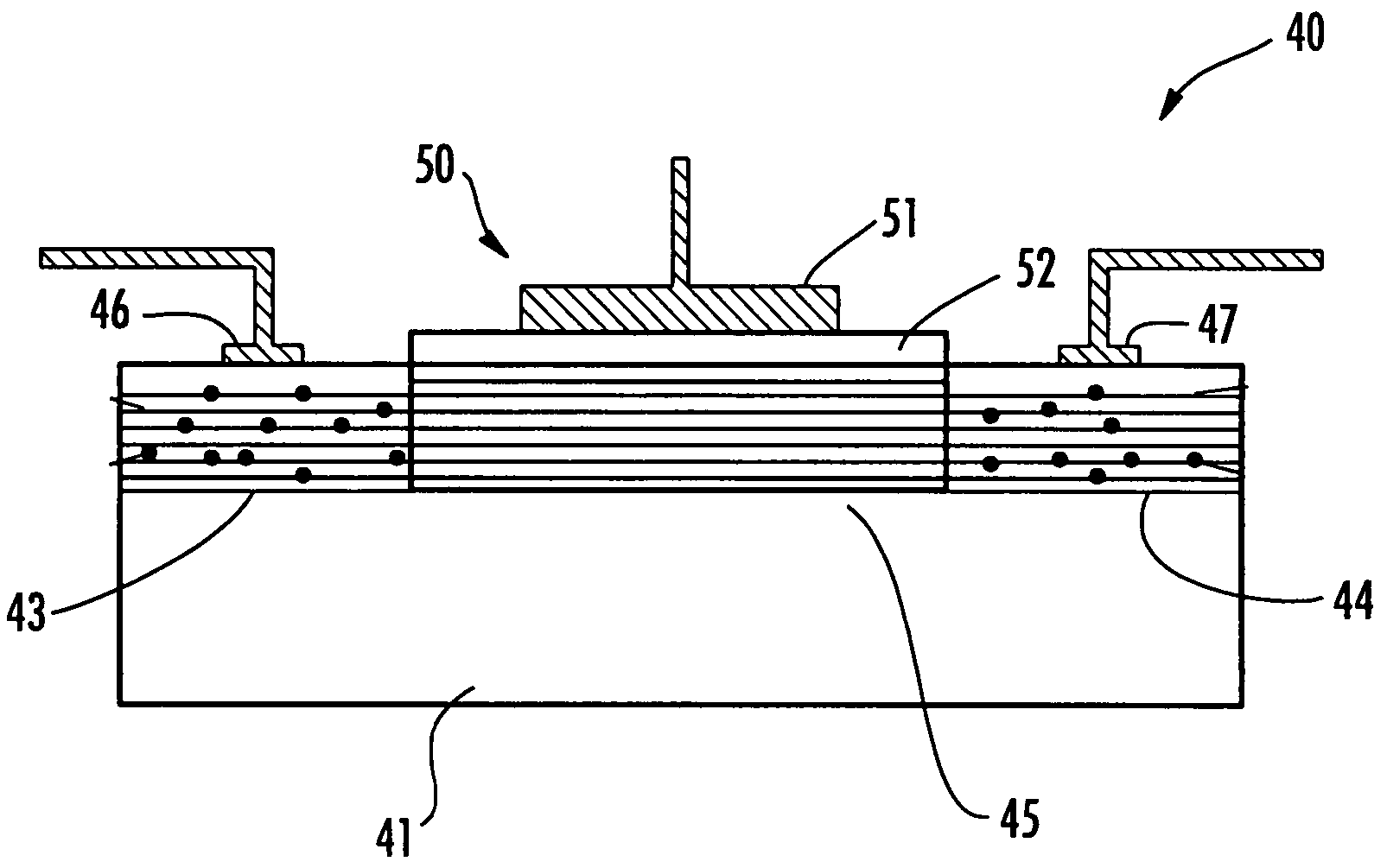
[0011]This and other objects, features and advantages in accordance with the present invention are provided by method for making a spintronic device comprising forming at least one superlattice and forming at least one electrical contact coupled thereto, with the at least one superlattice comprising a plurality of groups of layers. Each group of layers may comprise a plurality of stacked base semiconductor monolayers defining a base semiconductor portion having a crystal lattice, at least one non-semiconductor monolayer constrained within the crystal lattice of adjacent base semiconductor portions, and a spintronic dopant. Moreover, the spintronic dopant may be constrained within the crystal lattice of the base semiconductor portion by the at least one non-semiconductor monolayer. Accordingly, a fairly high spintronic dopant concentration may be achieved and maintained while reducing a likelihood of precipitation of the spintronic dopant.

Problems solved by technology

The article discloses four essential requirements for implementing a semiconductor spintronics technology in devices, and provides that the efficient electrical injection of spin-polarized carriers into the semiconductor has been a critical issue severely hampering progress in this field.
Current spintronics technology is limited by the currently used materials.
Although this may have a large spin polarization at the Fermi level and a large magnetoresistance effect and Curie temperature higher than in the bulk, it may suffer from a low thermal stability.
Unfortunately, many of the materials and structures for spintronic devices have relatively low concentrations of the spintronic dopant, such as Mn.

Method used


Image

  • Methods of making spintronic devices with constrained spintronic dopant
  • Methods of making spintronic devices with constrained spintronic dopant
  • Methods of making spintronic devices with constrained spintronic dopant

Examples


Embodiment Construction

[0031]The present invention will now be described more fully hereinafter with reference to the accompanying drawings, in which preferred embodiments of the invention are shown. This invention may, however, be embodied in many different forms and should not be construed as limited to the embodiments set forth herein. Rather, these embodiments are provided so that this disclosure will be thorough and complete, and will fully convey the scope of the invention to those skilled in the art. Like numbers refer, to like elements throughout.

[0032]Referring now to FIGS. 6A and 6B, a first example of the present invention is now described. In the schematically illustrated DFH structure 20 of FIG. 6A, Oxygen is included in the Si superlattice also including a transition metal, such as Mn. As can be seen in the energy level diagram 21 of FIG. 6B, the Mn will have lower energy as it approaches the Oxygen layer. In other words, when the Mn atoms stick to the Silicon atoms, the structure is most en...


PUM


Abstract

A method is for making a spintronic device and may include forming at least one superlattice and at least one electrical contact coupled thereto, with the at least one superlattice including a plurality of groups of layers. Each group of layers may include a plurality of stacked base semiconductor monolayers defining a base semiconductor portion having a crystal lattice, at least one non-semiconductor monolayer constrained within the crystal lattice of adjacent base semiconductor portions, and a spintronic dopant. The spintronic dopant may be constrained within the crystal lattice of the base semiconductor portion by the at least one non-semiconductor monolayer. In some embodiments, the repeating structure of a superlattice may not be needed.

Description

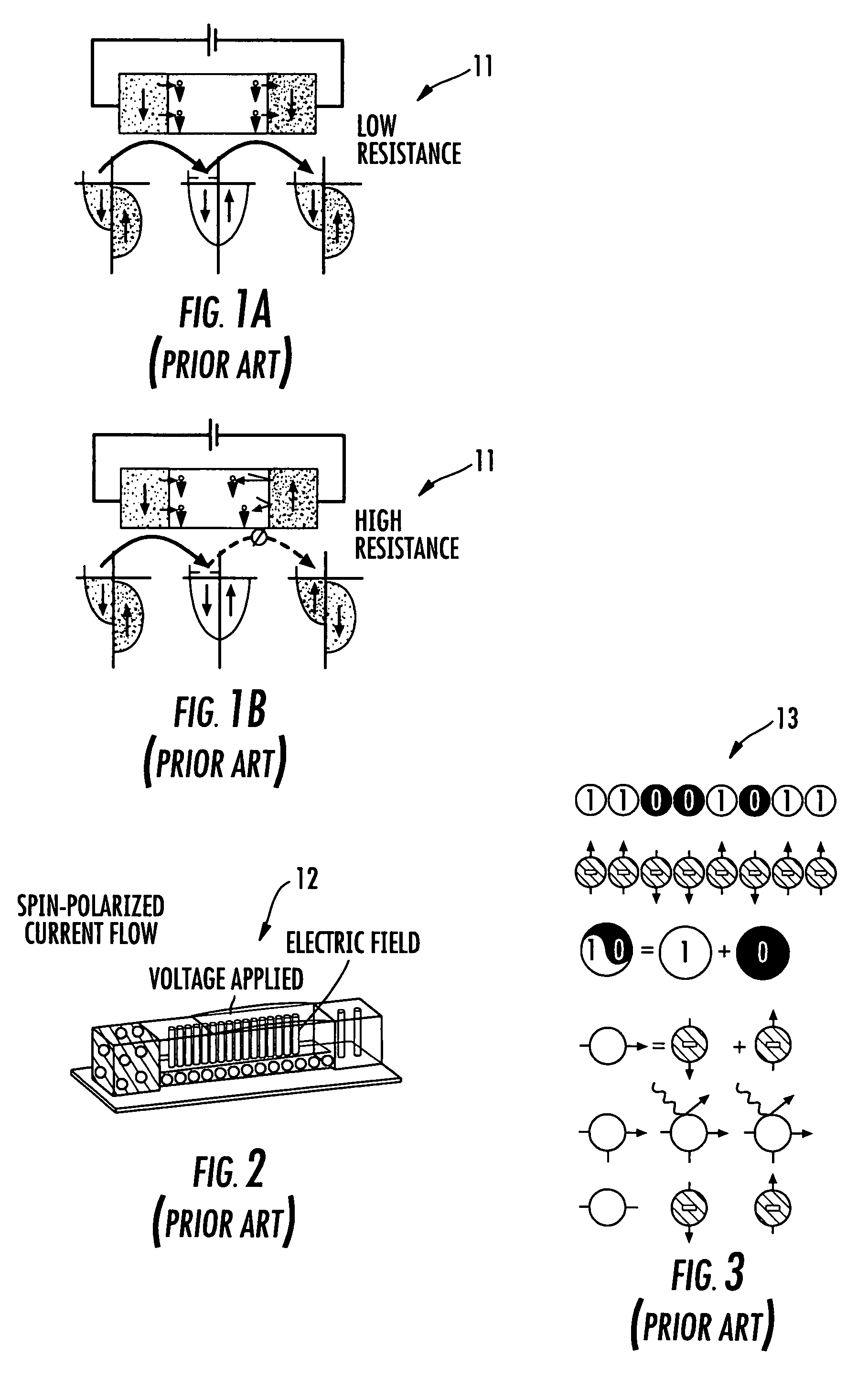
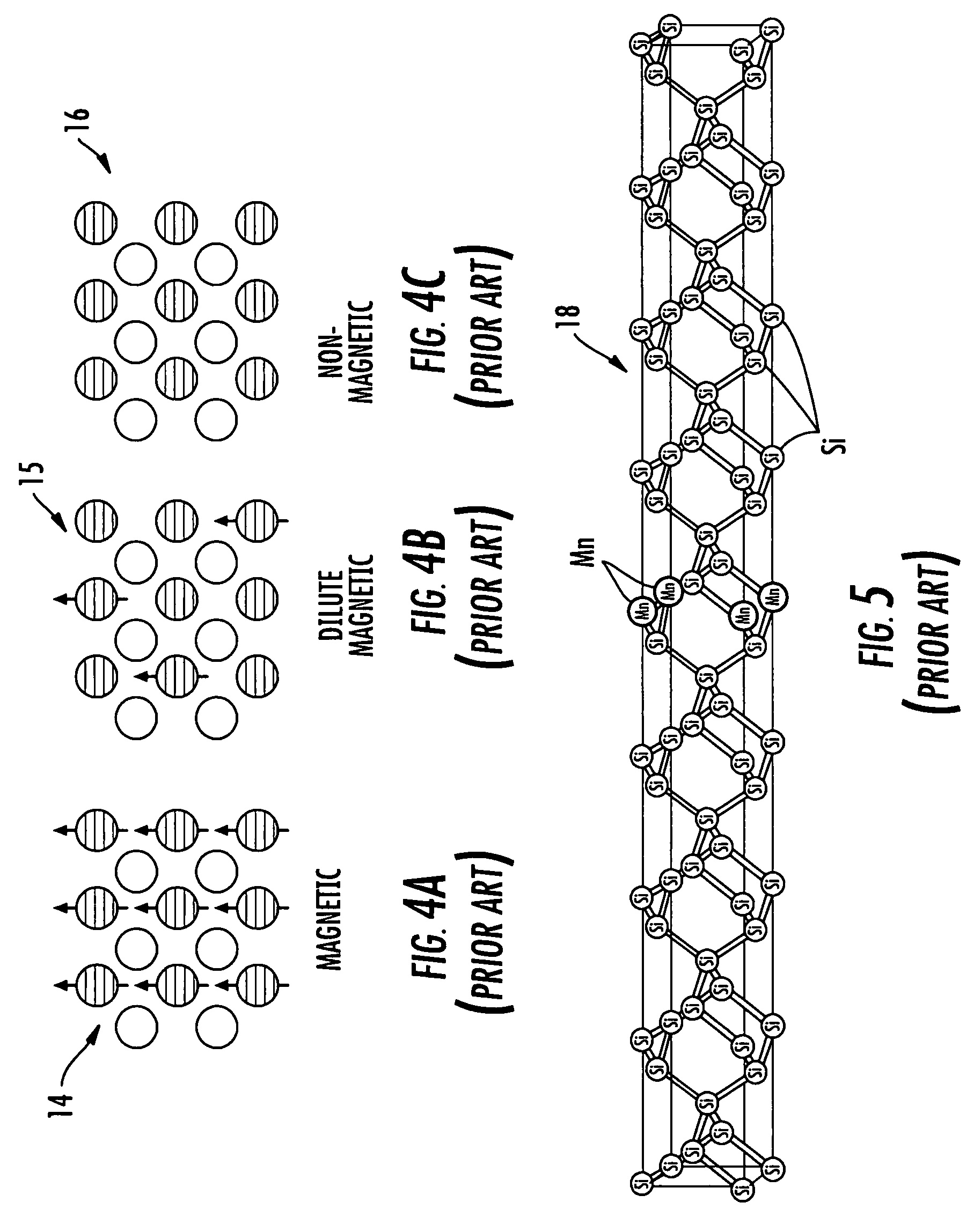
RELATED APPLICATION[0001]This application is based upon prior filed copending provisional application Ser. No. 60 / 783,598 filed Mar. 17, 2006, the entire subject matter of which is incorporated herein by reference in its entirety.FIELD OF THE INVENTION[0002]The present invention relates to the field of electronics, and, more particularly, to the field of spin-based electronics and associated methods.BACKGROUND OF THE INVENTION[0003]Spin-based electronics or spintronics exploit both the charge of electrons as well as the spin of the electrons to permit new devices with enhanced functions, higher speeds, and / or reduced power consumption, for example. An exemplary spintronic device is the spin valve as illustrated in the FIGS. 1A and 1B. The spin valve 11 provides a low resistance when the spins are aligned (FIG. 1A), and provides a high resistance with the spins not aligned (FIG. 1B). The spin valve 11 may be used as a nonvolatile memory element, for example. Other exemplary spintroni...

Claims


Application Information

Patent Timeline
Patent Type & Authority Patents(United States)
IPC IPC(8): H01L21/00
CPCB82Y10/00B82Y25/00B82Y40/00H01F1/401H01F10/3213H01F1/405H01F41/301H01L29/1054H01L29/15H01L29/66984H01F10/3268
Inventor HUANG, XIANGYANGHALILOV, SAMEDYIPTONG, JEAN AUGUSTIN CHAN SOW FOOKDUKOVSKI, ILIJAHYTHA, MAREKMEARS, ROBERT J.
Owner ATOMERA INC
Why Eureka
Try Eureka