
Apparatus and method for photo-electric measurement

a technology of photoelectric measurement and apparatus, applied in the field of apparatus and method for photoelectric measurement, can solve the problems of reducing device yield, sensitivity, and sensitivity, and limiting the size of the area that can be measured, and achieve the effect of less susceptible to dust and dirt, and mechanical stability

Inactive Publication Date: 2009-12-15
MILTENYI IMAGING GMBH
View PDF22 Cites 15 Cited by
  • Summary
  • Abstract
  • Description
  • Claims
  • Application Information

AI Technical Summary

Benefits of technology

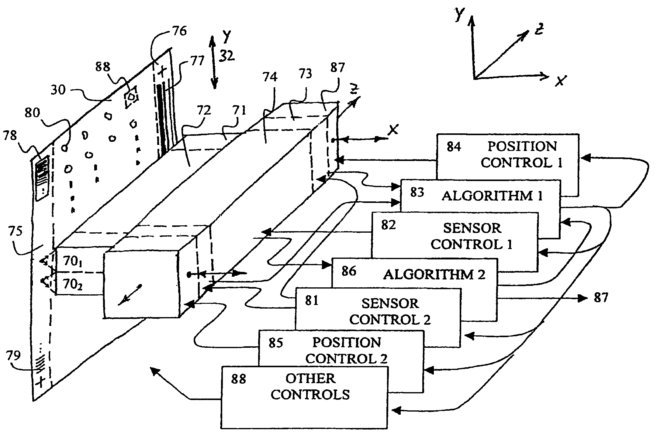
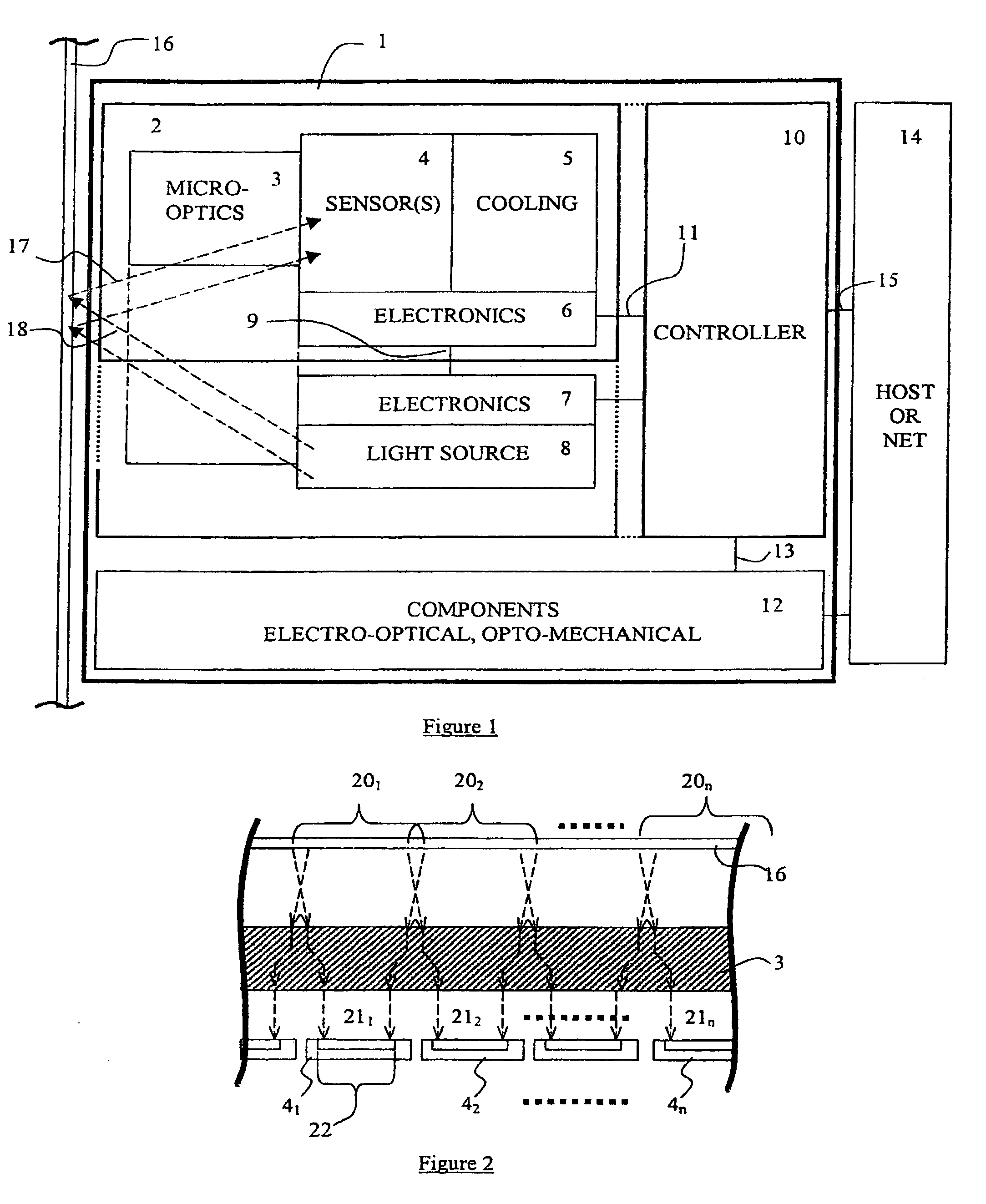
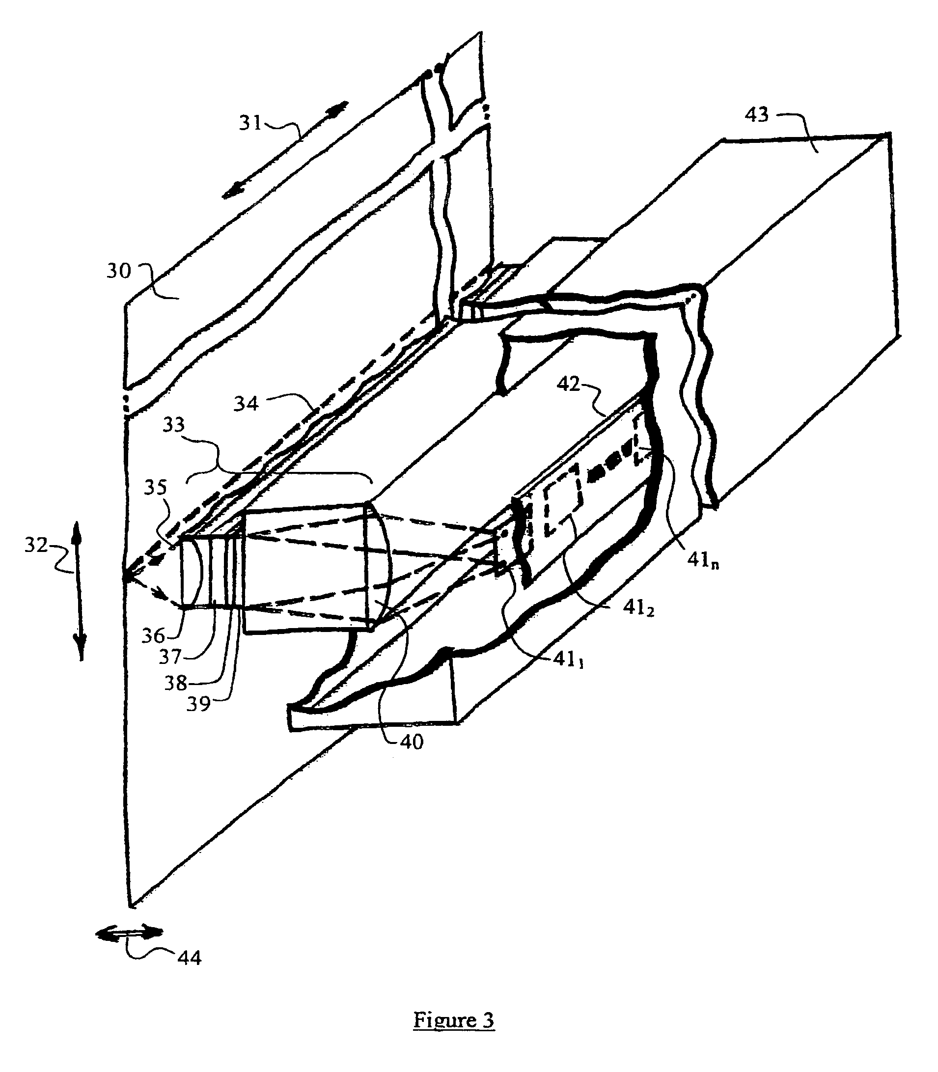
[0011]According to the present invention many smaller CCD devices are used in parallel instead of one large device. For example, as opposed to imaging an entire Microplate onto one large, expensive CCD, many smaller fields (perhaps each well) can be imaged at lower resolution. Smaller devices have less pixels—i.e., lower capacitances—and are inherently capable of running faster. Through the parallel readout of many devices, overall throughput is greatly increased—even if the readout rate is reduced in order to decrease noise. Smaller devices have higher production yields, and as mentioned above, less expensive optics can be used. By designing the parallelism modularly, the throughput can be indefinitely increased without speed penalty. In comparison to large devices, there is a limit to increasing the resolution, as the cost of the device increases. Speed (frame rate) decreases as the device gets larger. Since the areas to be imaged are very small and are typically spaced apart (e.g. in the 96-well plate), it is more efficient to use micro-optical arrays. In effect an array of objective lenses.
[0030]Compact, light detection unit suitable for mounting on moving robotic axes. The space required for the sensing unit in an optical system is minimal.

Problems solved by technology

a) Imaging, typically using cooled scientific CCD and CID cameras. Such array sensors have the inherent advantage of parallelism—that is, they allow the simultaneous measurement of a plurality of samples arranged on a plane surface. Spectral measurement is implemented by using interchangeable optical filters. The samples are typically illuminated or excited either simultaneously, or by scanning a light source over the area.
b) Scanning systems, typically involving the scanning of a laser over the sample carrier area, with measurement using one or more optical sensors such as Photomultiplier Tubes (PMT) or Avalanche Photodiodes. Spectral measurement is implemented either by using a number (n) of interchangeable optical filters with a single sensor, implying that the area to be measured must be scanned (n) times; or a plurality of sensors, each used with an optical filter. “Confocal” optical schemes, which limit the focal plane of measurement have been used with scanning systems to increase sensitivity, and to allow a third dimension of measurement in the “Z” or focal axis.
c) Scanning confocal systems which make use of an image sensor such as a CCD (Charge Coupled Device) are known. For example, WO 95 / 21378 discloses a scanning single-beam confocal apparatus for DNA sequencing, using a CCD-based spectrometer. WO 00 / 11024 is another such example where multiple laser beam excitation is employed with confocal multiple-spectra detection by a CCD sensor. Current instrumentation have limitations on the size of the area that can be measured, the resolution that can be achieved, and the speed of measurement. Furthermore, the performance and / or consistency of measurements vary with sample position over the area to be measured. Sensitivity decreases as the area (number of samples, throughput and speed) increases.
This has disadvantages of lower device yields and higher cost; slower readout rates due to the larger number of pixels; optical aberrations in standard imaging optics are increasingly problematic; and the inevitable resolution limit of semiconductor technology.
To perform spectroscopy, multiple images using various optical filters are acquired, leading to longer measurement time, and lower sensitivity.
Laser scanning systems also suffer from the same optical imaging problems caused by aberrations as the area as well as the resolution increases.
Demands increase on the precision of the mechanically scanning mirror, and reliability and robustness are issues at the relatively high scanning speeds.
The flatness and tilt of the surface or volume to be measured, as well as its positioning relative to the sensing system poses a problem as the area gets larger.
The resulting variation in focus within the measurement area leads to location-dependent performance.
In comparison to large devices, there is a limit to increasing the resolution, as the cost of the device increases.
There may be large “dead spaces” between the detection points.

Method used


Image

  • Apparatus and method for photo-electric measurement
  • Apparatus and method for photo-electric measurement
  • Apparatus and method for photo-electric measurement

Examples


third embodiment

[0075]Referring to the third embodiment in FIG. 10, a frame transfer type CCD may be used to acquire the two-sided spectral information. The active region 112 is exposed, then shifted quickly under the shaded region 113 (electronic shuttering action). As the shaded region is read via the serial register, the next exposure occurs in the active region.

[0076]Referring to the fourth embodiment in FIG. 11, a frame transfer type CCD with two shaded regions 116, 117 may be used to acquire the two-sided spectral information. The active region is divided into two separately controllable regions 114 and 115. In this case, two spectral orders can be measured simultaneously. Referring to the fifth embodiment in FIG. 12, two frame transfer type CCDs 118 and 119 may be used to acquire the two-sided spectral information.

sixth embodiment

[0077]Referring to the sixth embodiment in FIG. 13, the image sensor shown may be a full-frame or interline transfer type CCD, whereby one or two serial register(s) 120, 123 are positioned between the spectral orders to be measured. Light from the zeroth order is prevented from being collected by the sensor by a means such as an aluminium mask on the sensor, or by blocking the light off-chip; i.e. by blocking the light by means of a mechanical mask or aperture which is not integrated onto the photo-electric conversion device(s). The spectral halves 121, 122 may be recombined (binned) directly on-chip in the serial register during the readout process.

[0078]Referring to the sixth embodiment in FIG. 14, a frame transfer device may be used as described in relation to FIG. 13.

[0079]FIGS. 15 and 16 shows an embodiment of a means and a method of performing gated detection using image sensor(s). Such time gated fluorescence or luminescence measurements combined with spectral discrimination ...


PUM

PropertyMeasurementUnit
electricaaaaaaaaaa
lengthaaaaaaaaaa
areaaaaaaaaaaa

Abstract

An apparatus and a method for photo-electric measurement is included; the apparatus comprises photo-electric conversion devices and an optical system which is modularly expandable in order to acquire electromagnetic radiation from a line or area of any desired size on an object. The optical system preferably separates the electromagnetic radiation modularly into a plurality of smaller segments and projects electromagnetic radiation corresponding to the smaller segments onto individual photo-electric conversion devices and sensor electronics related to said photo-electric conversion device(s). This enables the operating mode and functionality of said photo-electric conversion device(s) to be defined and changed in real-time, whereby functions such as the readout sequence of pixels and unlimited flexibility of pixel binning in two dimensions are fully programmable, and the photo-electric conversion device(s) can operate and / or be controlled independently and / or simultaneously.

Description

BACKGROUND OF THE INVENTION[0001]Optical imaging combined with spectroscopy is commonly used for the analysis and testing of substances and materials, such as chemicals, molecules, cells, tissue, and the like, and for measurement / detection of related reactions, processes and events. These substances or processes may be arranged in units, hereto referred to collectively as “samples”, in order to facilitate handling and analysis. In order to increase speed, throughput, efficiency and to decrease cost, increasingly large numbers of samples are analyzed simultaneously in parallel, or alternatively in a high-speed serialized fashion, or a combination thereof. In many applications, a plurality of samples to be measured are prepared and organized such that they can be analyzed in an automated fashion, whereby they are placed in or on a “sample carrier”, typically in the format of an array. The sample carrier facilitates the handling, transport and processing of samples. In addition to the ...

Claims


Application Information

Patent Timeline
Patent Type & Authority Patents(United States)
IPC IPC(8): G01J3/26G01J3/28G01N21/31
CPCG01N21/31G01J3/2803
Inventor HING, PAUL ANTHONY
Owner MILTENYI IMAGING GMBH
Learn More