Clock signal generation circuit and semiconductor device

a clock signal and semiconductor technology, applied in the field of circuits, can solve the problems of semiconductor device malfunction, difficulty in obtaining a stable clock signal, frequency of a clock signal not reaching a stable value, etc., and achieve the effect of stable clock signal and low cos

Inactive Publication Date: 2009-12-29
SEMICON ENERGY LAB CO LTD
View PDF11 Cites 15 Cited by
  • Summary
  • Abstract
  • Description
  • Claims
  • Application Information

AI Technical Summary

Benefits of technology

[0008]A semiconductor device which transmits and receives data by a wireless signal requires very high performance, such as extension of communication distance, low power consumption, miniaturization of chips, and high reliability of encoding communication. For the extension of communication distance, for example, a wireless signal of a UHF band (915 MHz) can be used. Because the wireless signal of a UHF band can be used to perform long-distance communication in principle, compared with a wireless signal of an HF band, the wireless signal of a UHF band has an advantageous effect for extension of communication distance. However, when a communication signal of a UHF band is used, there are many problems in circuit design, such as generation of a stable clock signal in the semiconductor device; therefore, it is necessary to dramatically review the design of an HF wireless communication CPU.
[0010]In view of the foregoing problems, an object of the present invention is to provide a semiconductor device which operates stably at low cost by providing a clock signal generation circuit that can supply a stable clock signal.
[0021]According to the present invention, a clock signal generation circuit which can generate a stable clock signal and which operates stably and a semiconductor device provided with the clock signal generation circuit can be provided at low cost.

Problems solved by technology

However, when a communication signal of a UHF band is used, there are many problems in circuit design, such as generation of a stable clock signal in the semiconductor device; therefore, it is necessary to dramatically review the design of an HF wireless communication CPU.
However, in the case where a PLL circuit is mounted on a semiconductor device which transmits and receives data by a wireless signal, it is difficult to obtain a stable clock signal.
In addition, there is a case where a frequency of a clock signal does not reach a stable value during the synchronous period.
Although these are caused by variations in the characteristics of chips in a manufacturing process, these mean that the frequency of a clock signal is changed or set to be at a non-specified value, which causes a malfunction of the semiconductor device.
Furthermore, the semiconductor device which transmits and receives data by a wireless signal is required to be provided at low cost; therefore, an expensive manufacturing process cannot be applied indiscriminately.

Method used


Image

  • Clock signal generation circuit and semiconductor device
  • Clock signal generation circuit and semiconductor device
  • Clock signal generation circuit and semiconductor device

Examples


embodiment mode 1

[0039]A clock signal generation circuit of the present invention will be described in this embodiment mode.

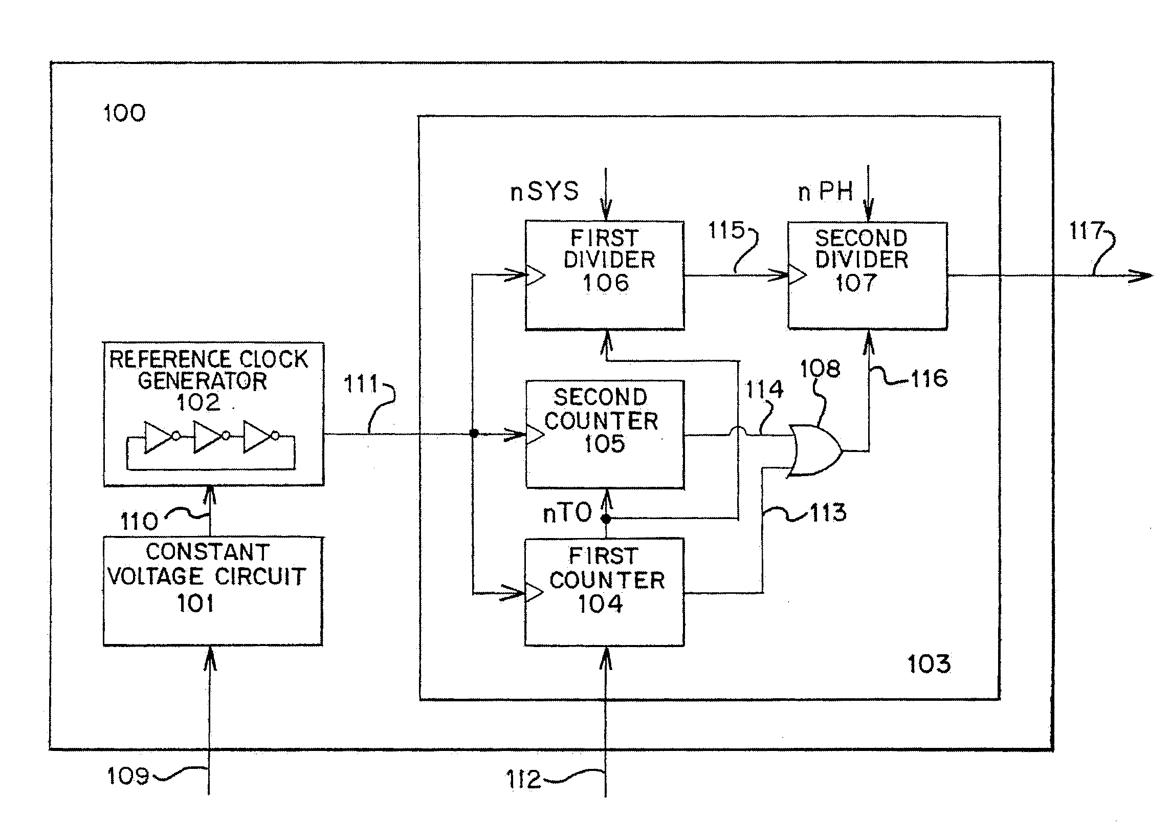
[0040]A block diagram of a clock signal generation circuit of the present invention is shown in FIG. 1. In FIG. 1, a clock signal generation circuit (also referred to as a clock generator) 100 includes a constant voltage circuit (also referred to as a regulator) 101, a reference clock signal generation circuit 102, and a counter group 103. The counter group 103 includes a first counter circuit 104, a second counter circuit 105, a first divider circuit 106, a second divider circuit 107, and a reset signal generation circuit 108.

[0041]Next, a connection relationship of each structure in the clock signal generation circuit 100 will be described.

[0042]The constant voltage circuit 101 is connected to the reference clock signal generation circuit 102. The reference clock signal generation circuit 102 is connected to the first counter circuit 104, the second counter circuit 105, and t...

embodiment mode 2

[0072]In this embodiment mode, a semiconductor device provided with the clock signal generation circuit described in Embodiment Mode 1 will be described.

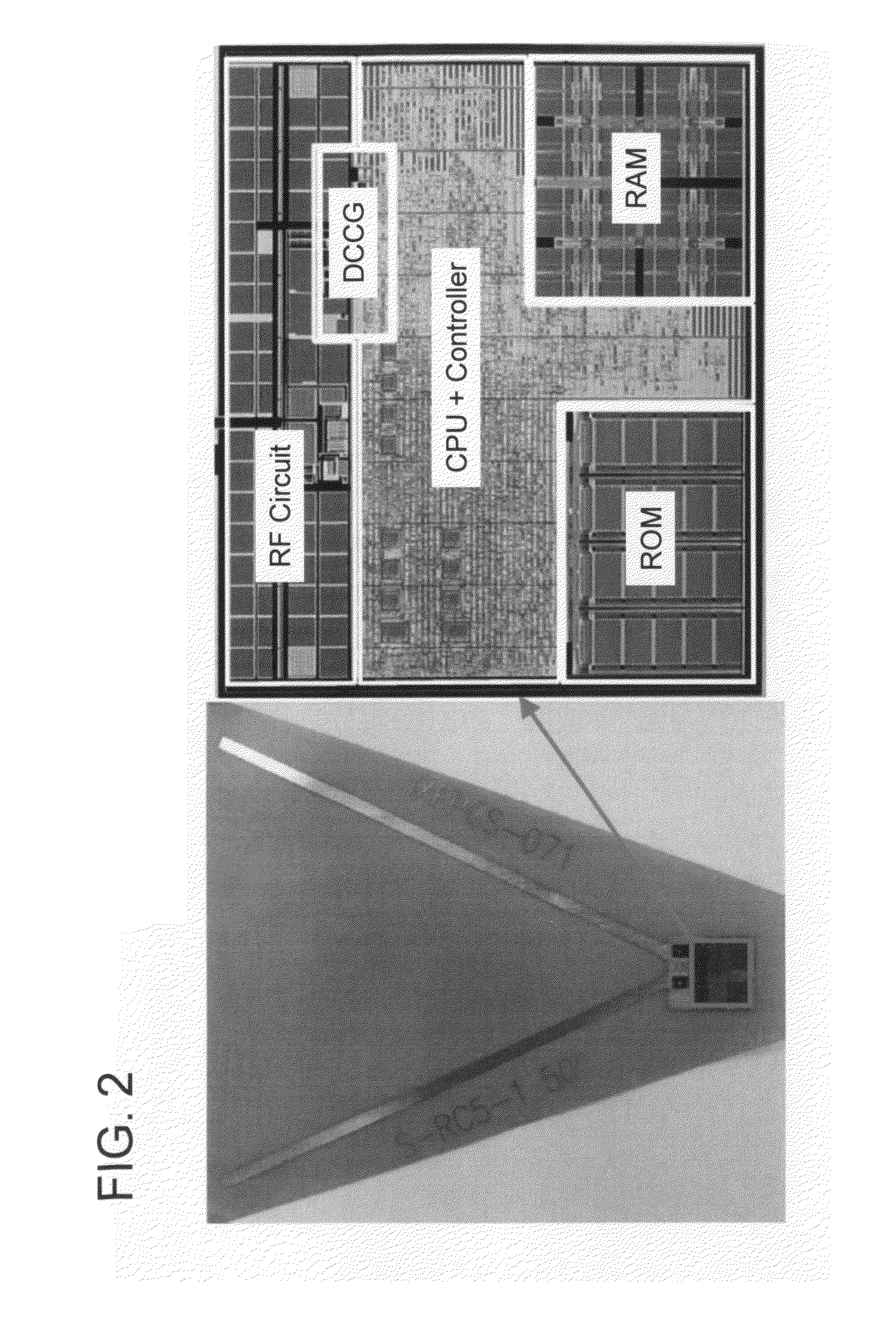
[0073]A structure of the semiconductor device of this embodiment mode is shown in FIG. 3. A semiconductor device 300 includes an RF circuit 301, a clock signal generation circuit 302, a logic circuit 303, and an antenna 317 in an antenna portion 318. Note that, although not shown in FIG. 3, the semiconductor device 300 transmits and receives a wireless signal to and from an external circuit such as a wireless communication device via the antenna 317.

[0074]Next, a structure of each circuit will be described. The RF circuit 301 includes a power supply circuit 304, a demodulation circuit 305, and a modulation circuit 306. The clock signal generation circuit 302 includes a constant voltage circuit 307, a ring oscillator 308, and a counter group 309. In addition, the logic circuit 303 includes a controller 313, a CPU (also referred to as...

embodiment mode 3

[0082]In this embodiment mode, one example of a method for manufacturing a semiconductor device described in the above embodiment mode will be described. In this embodiment mode, a structure in which a semiconductor device including an antenna circuit is provided over the same substrate will be described.

[0083]First, as shown in FIG. 9A, an insulating film 1902 is formed over one surface of a substrate 1901, and a peeling layer 1903 is formed over the substrate 1901 with the insulating film 1902 interposed therebetween, and then an insulating film 1904 functioning as a base film and a semiconductor film 1905 (e.g., a film containing amorphous silicon) are formed thereover. Note that the insulating film 1902, the peeling layer 1903, the insulating film 1904, and the semiconductor film 1905 can be formed consecutively.

[0084]The substrate used for the substrate 1901 is selected from a glass substrate, a quartz substrate, a ceramic substrate, a metal substrate (e.g., a stainless steel s...


PUM


Abstract

The semiconductor device is provided with a clock signal generation circuit that includes a reference clock signal generation circuit which generates a first reference clock signal, a first counter circuit which counts the number of rising edges of the first reference clock signal by using the first reference clock signal and a synchronizing signal, a second counter circuit which counts the number of rising edges of the first reference clock signal by using an enumerated value of the first counter circuit, a first divider circuit which divides a frequency of the first reference clock signal by using the enumerated value of the first counter circuit and generates a second reference clock signal, and a second divider circuit which divides a frequency of the second reference clock signal and generates a clock signal.

Description

BACKGROUND OF THE INVENTION[0001]1. Field of the Invention[0002]The present invention relates to a circuit that generates a clock signal. In addition, the present invention relates to a semiconductor device provided with a circuit that generates such a clock signal.[0003]2. Description of the Related Art[0004]In recent years, a semiconductor device in which an ultra-small IC chip and an antenna for wireless communication are combined with each other (also referred to as an RFID tag, a wireless tag, an ID tag, or an RF tag) has been attracting attention. The semiconductor device can transmit and receive data without contact, for example, it can write data or read data, by transmission and reception of a communication signal by use of a wireless communication device (which can communicate wirelessly, for example, a reader / writer, a cellular phone, a personal computer, or the like).[0005]As an application field of a semiconductor device which transmits and receives data by a wireless s...

Claims


Application Information

Patent Timeline
Patent Type & Authority Patents(United States)
IPC IPC(8): G06F1/04H03K3/00
CPCG06F1/025H04L7/033G06F7/68G06F1/04G11C7/22G11C7/10G11C7/20
Inventor KUROKAWA, YOSHIYUKIIKEDA, TAKAYUKIENDO, MASAMIDEMBO, HIROKIKAWAE, DAISUKEINOUE, TAKAYUKIKOZUMA, MUNEHIRO
Owner SEMICON ENERGY LAB CO LTD
Why Eureka
Try Eureka