Polymer enhanced cholesteric electro-optical devices

a technology of electrooptical devices and cholesteric acid, which is applied in the direction of thin material processing, instruments, chemistry apparatuses and processes, etc., can solve the problems of increasing the difficulty of manufacturing process, increasing power consumption, and deficient motion picture response time, and achieve high contrast in-plane switching

Inactive Publication Date: 2010-01-26
KENT STATE UNIV
View PDF14 Cites 16 Cited by
  • Summary
  • Abstract
  • Description
  • Claims
  • Application Information

AI Technical Summary

Benefits of technology

[0008]It is therefore, an aspect of the present invention to provide liquid crystal devices comprised of a composite of an internal polymer network localized on one or more substrate surfaces and short-pitch cholesteric liquid crystal having a positive dielectric anisotropy that can be employed to operate in different modes, such as, in-plane switching (frequency modulation) and out-of-plane switching (phase modulation). It is likewise an aspect of the present invention to provide a method of making a liquid crystal device that comprises the internal spatially ordered polymer network localized on the surface of the substrate. In this context, “localized on the surface” refers to a polymer network which is concentrated at the surface of the substrate of a liquid crystal cell and wherein the bulk of the cell has a relatively lower concentration of the polymer network, and more specifically, wherein the bulk may be relatively or substantially free from the polymer network, i.e. having less than about 25%, or preferably less than about 10% polymer network through the center of the cholesteric film. The invention is related to a method for localized stabilization of the ULH texture of a short pitch cholesteric liquid crystal by means of a polymer network created at the substrate interface with the cholesteric by means of photo polymerization of a photo reactive monomer dissolved into the cholesteric liquid crystal material. Furthermore, the present invention has the advantage over the known prior art which uses the flexoelectro-optical effect of liquid crystal of providing high contrast in-plane switching.

Problems solved by technology

Traditional LCDs are based on nematic technologies which are still deficient in response time for perfect motion picture viewing.
However, the approach of using thinner cell gap increases the difficulty in the manufacturing process.
In addition, using higher switching voltage to address the LCDs increases the power consumption.
However, the flexoelectric-optical effect vanishes upon shutting down the device and therefore requires a warm-up period to achieve the threshold voltage.
However, the stabilization of ULH texture by polymer network proposed by Rudquist et al resulted in a residual birefringence of the completely unwound cholesteric texture due to the morphology of the polymeric network formed into the bulk of the cholesteric liquid crystal by means of photopolymerisation of 10 wt % photoreactive monomer dissolved in the cholesteric liquid crystal.
The residual birefringence in turn decreased the contrast of the cell optical appearance at applied electric field higher than the threshold one for unwinding of helical axis thus affecting severely the efficiency of the modulation in the cell birefringence due to the field induced helix unwinding.
Moreover, the dense polymer network stabilizing the ULH texture of the cholesteric reported by Rudquist et al negatively affects the cell performance in the degree of the light intensity modulation as well as the switching time.
In addition, device that operates in polar (flexoelectric) as well as quadratic, with the applied electric field (helix unwinding), mode has not been realized yet.
However, the out-of-plane dielectric coupling hinders the large in-plane rotation of axis from minimum to the maximum light transmittance and hence, the optical contrast.

Method used


Image

  • Polymer enhanced cholesteric electro-optical devices
  • Polymer enhanced cholesteric electro-optical devices
  • Polymer enhanced cholesteric electro-optical devices

Examples


example 1

Preparation and Characterization of a Liquid Crystal Cell

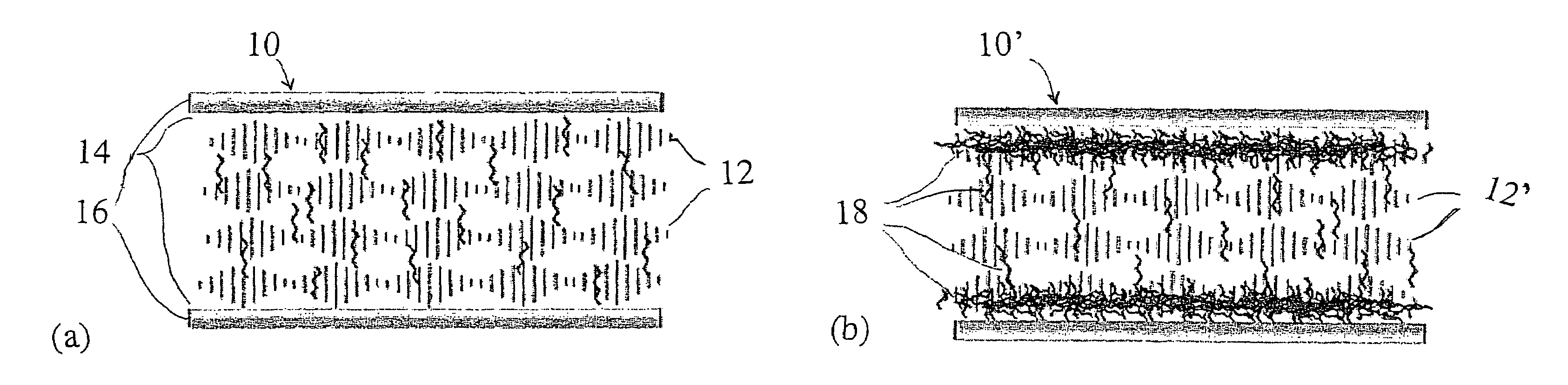
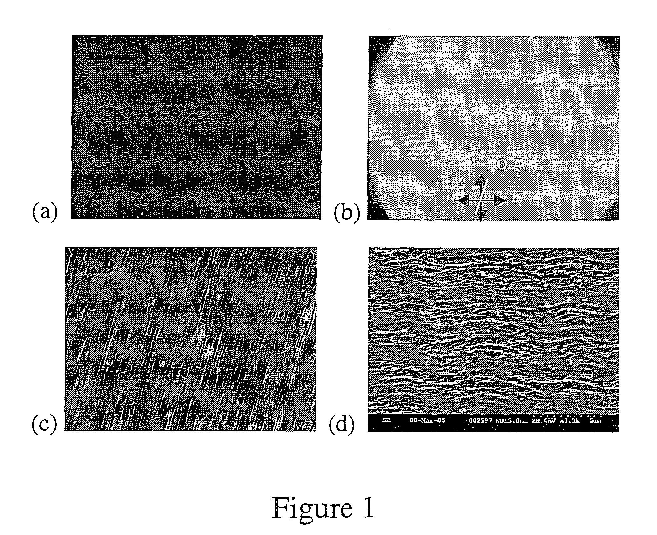
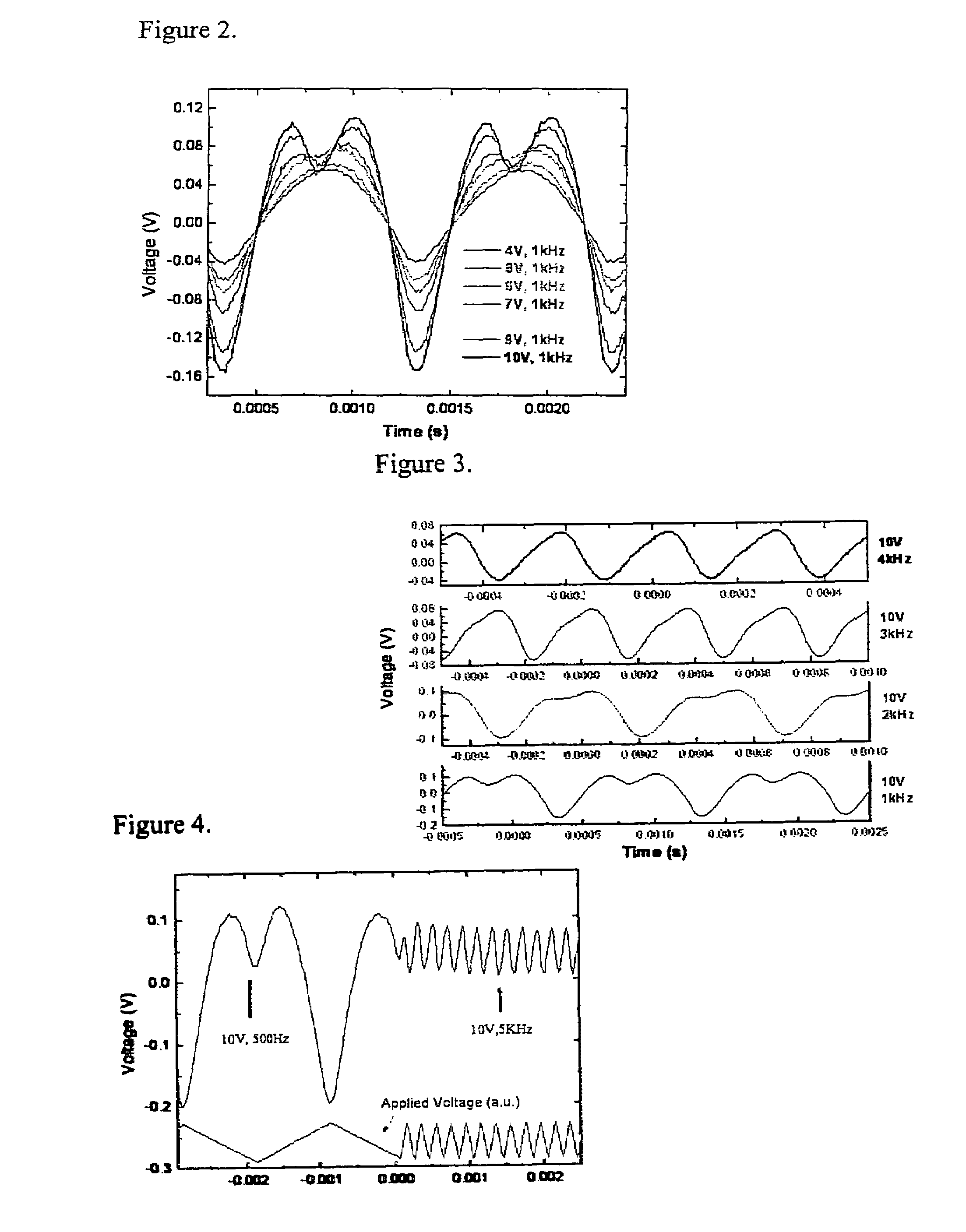
[0024]The mesogenic monomer RM257 was added to ChLC and the mixture was vortex-mixed in a vial, heated to around 50° C. and cooled to room temperature. Commercial electro-optical cells with ITO electrodes (i.e. having an electrode area ˜10 mm2) and alignment layers deposited on the inner surface of the confining substrates and with μm spacers are used for a planar alignment. The mixture is sandwiched between two substrates with patterned electrodes and alignment layers deposited on the electrodes and rubbed and assembled in a fashion to provide homogeneous alignment. Glass spacers were used in order to control the uniformity of cell gap. The cell was heated to a high temperature exceeding the isotropic temperature of the mixture and cooled to room temperature either with 2.7 V / μm @ 1 KHz or without an applied voltage. Once such a texture was obtained, the cell is exposed to UV light at 0.8 mW / cm2 intensity for 5 min at room te...


PUM

PropertyMeasurementUnit
wave lengthaaaaaaaaaa
electric fieldaaaaaaaaaa
temperatureaaaaaaaaaa

Abstract

The present invention provides liquid crystal devices comprised of a composite of an internal polymer network localized on the substrate surfaces and short-pitch dual-frequency switchable cholesteric liquid crystal that operate in two different modes including in-plane switching (amplitude modulation) and out-of-plane switching (phase modulation). The invention further provides a method of making a liquid crystal device demonstrating uniform lying helical axis where the device comprises a composite of an internal spatially ordered polymer network localized by in-situ photo-polymerization at the surface of the substrate. The invention can be used for flat panel displays, as well as spatial light modulators for applications such as optical waveguides, optical beam scanners, computer-generated holograms, and adaptive optics.

Description

FIELD OF THE INVENTION[0001]The invention relates to liquid crystal devices which include an internal polymer network localized to a substrate surface and a short-pitch cholesteric liquid crystal having a positive dielectric anisotropy that can be employed to operate in different modes, such as, in-plane switching (“IPS”, amplitude modulation) and out-of-plane switching (phase modulation). The present invention further relates to a method of making a liquid crystal device which includes the internal spatially ordered polymer network localized on the surface by in situ photopolymerization and which provides high contrast in-plane switching by using the flexoelectro-optical effect of the liquid crystal.BACKGROUND OF THE INVENTION[0002]The next generation liquid crystal displays (LCDs) will require LCDs with motion picture quality, ultra high contrast, brightness and wide viewing characteristics. Traditional LCDs are based on nematic technologies which are still deficient in response t...

Claims


Application Information

Patent Timeline
Patent Type & Authority Patents(United States)
IPC IPC(8): G02F1/1333C09K19/38C09K19/52
CPCC09K19/544C09K19/586G02F1/1334G02F1/13718Y10T428/10C09K2019/546C09K19/0258C09K2323/00
Inventor CHIEN, LIANG-CHYSHI, LEIKIM, SANG HWA
Owner KENT STATE UNIV
Why Eureka
Try Eureka