Multi-linearity mode LNA having a deboost current path

a multi-linearity mode and current path technology, applied in the field of low-noise amplifiers, can solve the problems of source-degenerated lnas, poor linearity, higher power consumption, etc., and achieve the effect of facilitating one current path tuning, low noise and less iteration

Active Publication Date: 2010-04-13
QUALCOMM INC
View PDF7 Cites 29 Cited by
  • Summary
  • Abstract
  • Description
  • Claims
  • Application Information

AI Technical Summary

Benefits of technology

[0011]A modified derivative superposition (MDS) low noise amplifier (LNA) includes a main current path and a cancel current path. In the main current path, a main current IMAIN flows through a load, through a main field effect transistor (FET), and through a first source degeneration inductor. In the cancel current path, a cancel current ICANCEL flows through the load, through a cancel FET, and through a second source degeneration inductor. The LNA current is the summation of IMAIN and ICANCEL. Third-order distortion in ICANCEL is used to cancel third-order distortion in IMAIN and therefore results in a zero third-order intermodulation distortion (IMD3) in the output current. In one novel aspect, the first source degeneration inductor in the main current path is a separate inductor form the second source degeneration inductor in the cancel current path, thereby facilitating tuning of one current path without affecting the other current path. As a result, the LNA can be optimized with less iteration because the main current and the cancel current are decoupled through the use of two separate source degeneration inductors.
[0012]In a second novel aspect, a deboost current path is provided. In the deboost current path, the deboost current IDEBOOST flows through a deboost transistor, and through the first source degeneration inductor. The deboost current does not flow through the LNA load. The deboost current allows more negative feedback to be provided by the first source degeneration inductor without decreasing the voltage headroom of the main FET. Therefore, higher linearity performance of the LNA can be achieved. In one example, the deboost current IDEBOOST can be changed during design of the LNA by changing the size of the deboost transistor. Accordingly, the negative feedback associated with the main current path can also be adjusted by adjusting the deboost current. The adjustability of the negative feedback factor provides extra tuning capability for optimal current cancellation. As a result, the LNA can be optimized with fewer design iterations.
[0013]In a third novel aspect, the LNA is programmable to operate in two different operational modes: a high linearity mode and a low linearity mode. When there is a receive jammer or a transmit leakage present, the LNA operates in the high linearity mode. In the high linearity mode, both the deboost current path and the cancel current path are enabled in order to achieve high linearity performance. On the other hand, when there is no receive jammer or transmit leakage present, the LNA operates in the low linearity mode. In the low linearity mode, the deboost current path is programmably disabled to reduce power consumption. In one example, the cancel current path is also disabled to improve the noise figure (NF) of the LNA.

Problems solved by technology

Source-degenerated LNAs, however, still suffer from poor linearity due to a second order non-linearity feedback effect.
Furthermore, LNAs with larger source degeneration inductances exhibit lower gain and higher noise factor, and the increasing of bias current causes higher power consumption.
If bias current is increased too much, then headroom problems are encountered.
However, the conventional DS method does not significantly increase IIP3 performance at high frequencies due to a second-order nonlinearity contribution to the third-order intermodulation distortion (IMD3).
The degree to which the bias current can be increased is, however, limited.

Method used


Image

  • Multi-linearity mode LNA having a deboost current path
  • Multi-linearity mode LNA having a deboost current path
  • Multi-linearity mode LNA having a deboost current path

Examples


Embodiment Construction

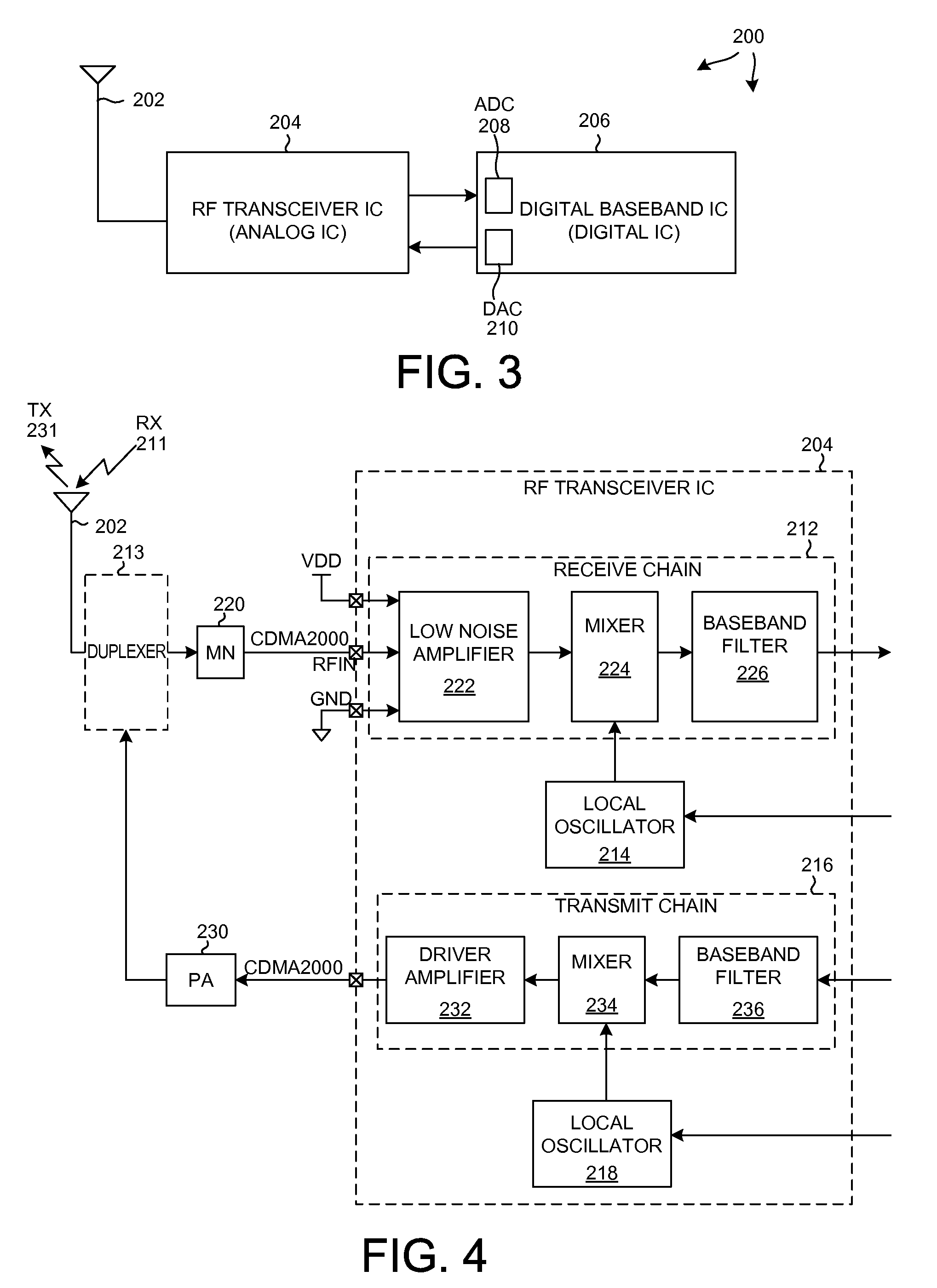
[0028]FIG. 3 is a very simplified high level block diagram of one particular type of mobile communication device 200 in accordance with one novel aspect. In this example, mobile communication device 200 is a cellular telephone that uses the CDMA 2000 cellular telephone communication protocol. The cellular telephone includes (among several other parts not illustrated) an antenna 202 and two integrated circuits 204 and 206. Integrated circuit 206 is called a “digital baseband integrated circuit” or a “baseband processor integrated circuit”. Integrated circuit 204 is an RF transceiver integrated circuit. RF transceiver integrated circuit 204 is called a “transceiver” because it includes a transmitter as well as a receiver.

[0029]FIG. 4 is a more detailed block diagram of the RF transceiver integrated circuit 204 of FIG. 3. The receiver includes what is called a “receive chain”212 as well as a local oscillator (LO) 214. When cellular telephone 200 is receiving, a high frequency RF signal...


PUM


Abstract

A modified derivative superposition (MDS) low noise amplifier (LNA) includes a main current path and a cancel current path. Third-order distortion in the cancel path is used to cancel third-order distortion in the main path. In one novel aspect, there is a separate source degeneration inductor for each of the two current paths, thereby facilitating tuning of one current path without affecting the other current path. In a second novel aspect, a deboost current path is provided that does not pass through the LNA load. The deboost current allows negative feedback to be increased without generating headroom problems. In a third novel aspect, the cancel current path and / or deboost current path is programmably disabled to reduce power consumption and improve noise figure in operational modes that do not require high linearity.

Description

BACKGROUND INFORMATION[0001]1. Technical Field[0002]The disclosed embodiments relate generally to wireless communication devices and, more specifically, to low noise amplifiers.[0003]2. Background Information[0004]Radio receivers, such as Code Division Multiple Access (CDMA) cellular telephone receivers, generally include amplifiers called low noise amplifiers (LNAs). The CDMA cellular telephone application requires that the LNAs have a very high third-order input intercept point (IIP3) as well as a low noise factor (NF), a high gain, and a low current consumption. There are several linearization techniques that are used to achieve these performance characteristics.[0005]One popular technique involves the use of negative feedback. In a conventional source-degenerated LNA, a source degeneration inductor is used as a feedback circuit. In general, higher linearity may be achieved by increasing the source degeneration inductance and / or by increasing the LNA bias current. Source-degenera...

Claims


Application Information

Patent Timeline
Patent Type & Authority Patents(United States)
IPC IPC(8): H03F3/04H03G3/12
CPCH03F1/223H03F1/3205H03F3/72H03F1/3252H03F2200/492
Inventor CHANG, LI-CHUNG
Owner QUALCOMM INC
Why Eureka
Try Eureka