

Fabrication method of GaN power LEDs with electrodes formed by composite optical coatings
a technology of composite optical coating and gan power led, which is applied in the direction of semiconductor photoelectronic devices, electrical equipment, basic electric elements, etc., can solve the problems of degrading the extraction efficiency of led and long way to achieve, and achieves the effects of improving luminous efficiency, high density, and simplifying the process
- Summary
- Abstract
- Description
- Claims
- Application Information
AI Technical Summary
Benefits of technology
Problems solved by technology
Method used
Image

Examples
Embodiment Construction
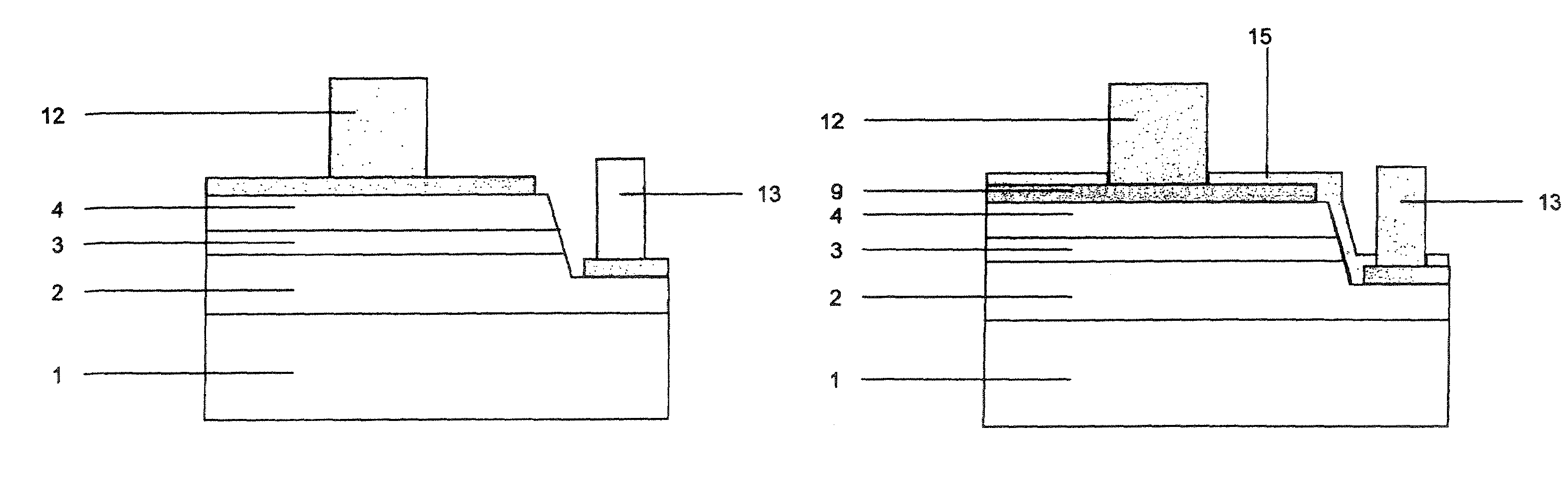
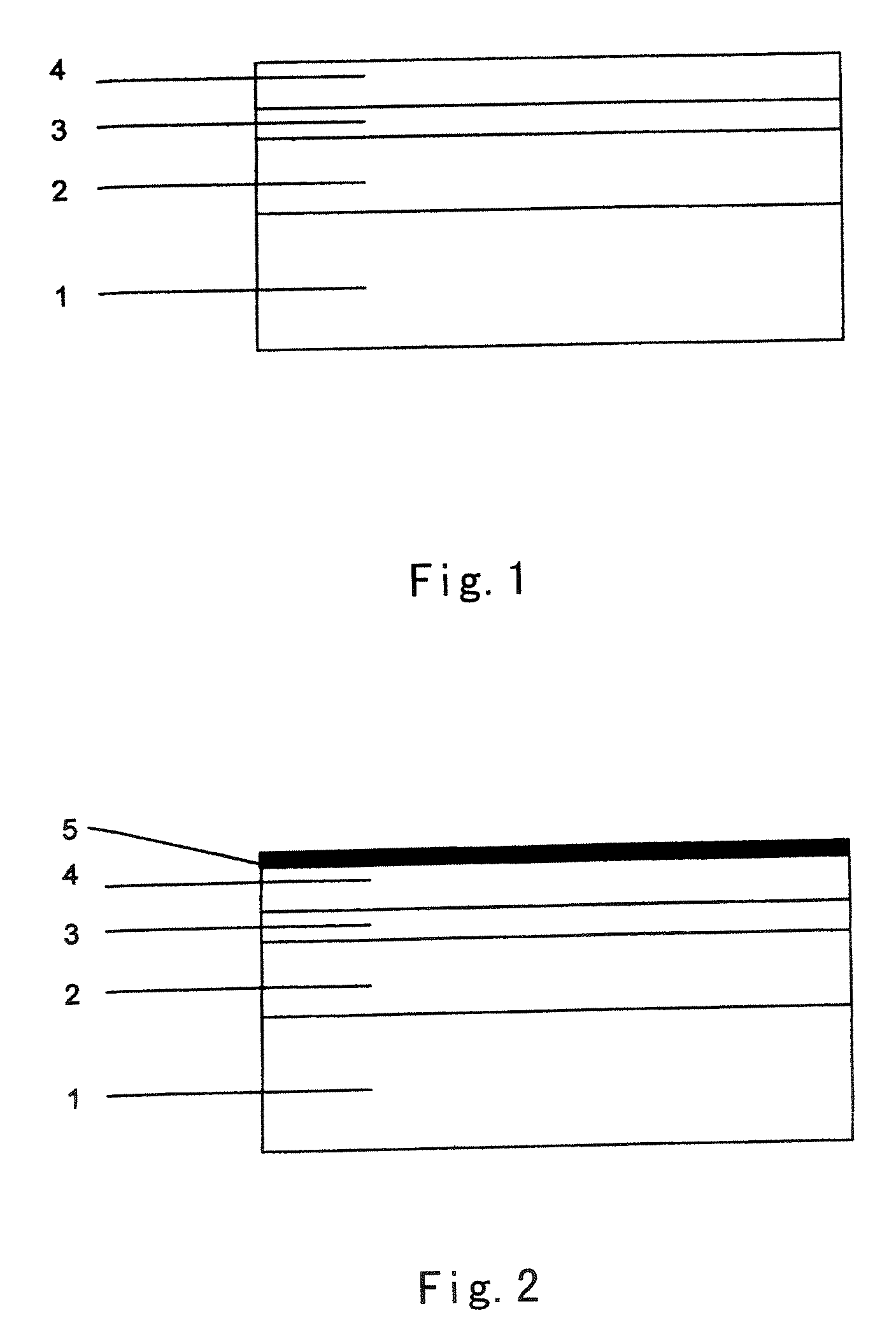
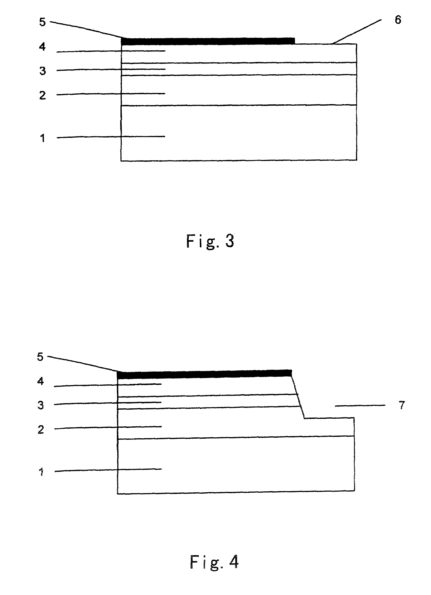
[0041]The invention will be depicted with reference to FIGS. 1-10, which illustrates a fabrication method of GaN power LED with electrodes formed by composite optical coatings, characterized by comprising the steps of:[0042]a) epitaxially growing an N—GaN layer 2, an active layer 3, a P—GaN layer 4 successively on a substrate 1 (see FIG. 1);[0043]b) depositing a mask layer 5 of SiO2 on the P—GaN layer 4 by a PECVD process (see FIG. 2);[0044]c) coating the mask layer 5 with photoresist, and then etching the mask layer 5 into an N—GaN electrode pattern 6 by photolithography process and wet etching (see FIG. 3);[0045]d) removing the remaining portion of the photoresist, and then forming an N—GaN electrode region 7 by etching through the N—GaN electrode pattern 6 by ICP dry etching (see FIG. 4);[0046]e) removing the remaining portion of the mask layer 5 by wet etching process, and then cleaning (see FIG. 5);[0047]f) simultaneously forming a transparent and electrically conductive film, ...
PUM
| Property | Measurement | Unit |
|---|---|---|
| pressure | aaaaa | aaaaa |
| temperature | aaaaa | aaaaa |
| transparent | aaaaa | aaaaa |
Abstract
Description
Claims
Application Information