Method and structures for highly efficient hot carrier injection programming for non-volatile memories

a non-volatile memory, high-efficiency technology, applied in the direction of digital storage, instruments, semiconductor devices, etc., can solve the problems of low programming efficiency, difficult charge pump circuit design, and inability to meet the requirements of the charge pump, so as to improve the programming efficiency, and reduce the current of the devi

Active Publication Date: 2010-06-08
PEGASUS SEMICON SHANGHAI CO LTD
View PDF8 Cites 21 Cited by
  • Summary
  • Abstract
  • Description
  • Claims
  • Application Information

AI Technical Summary

Benefits of technology

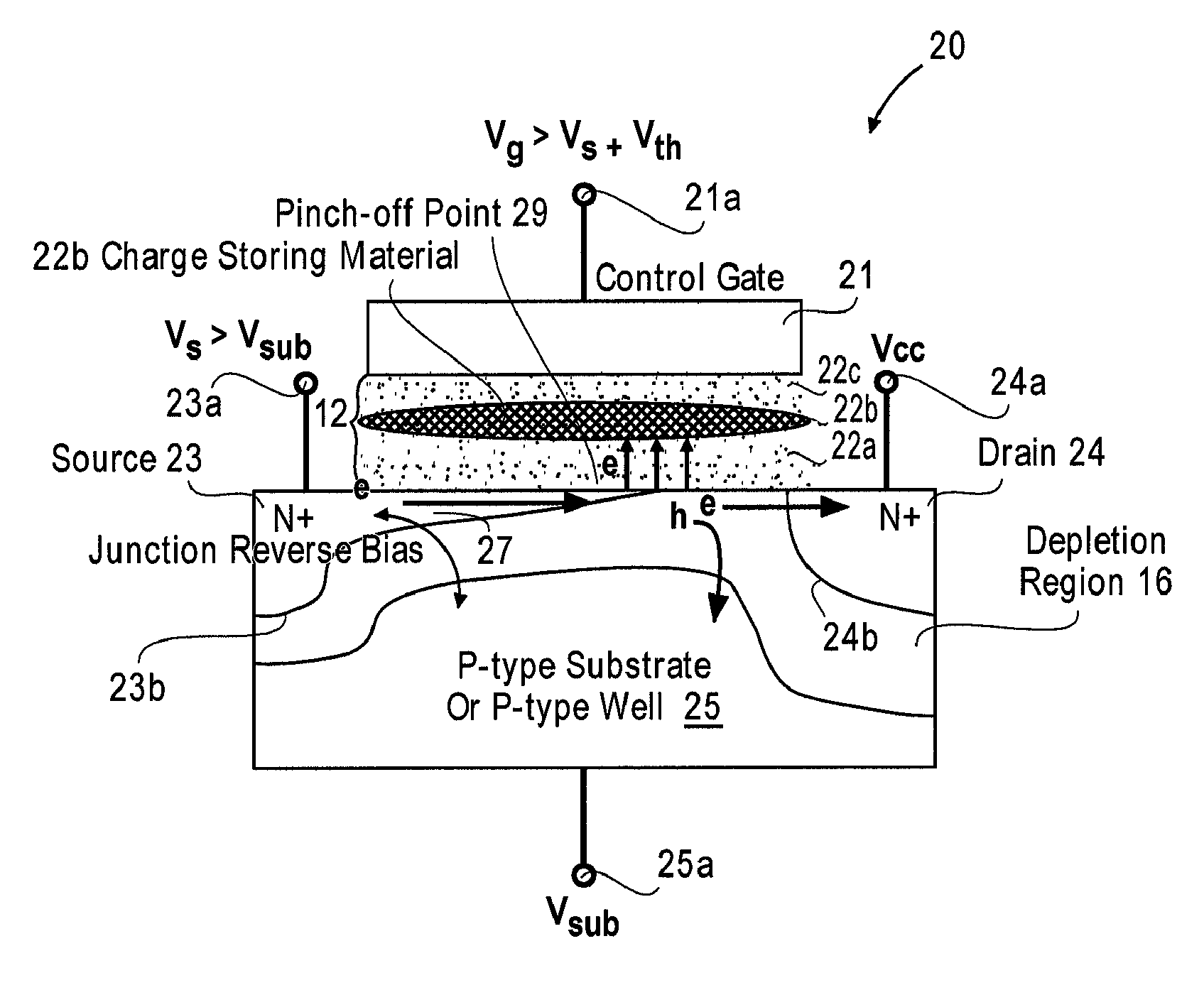
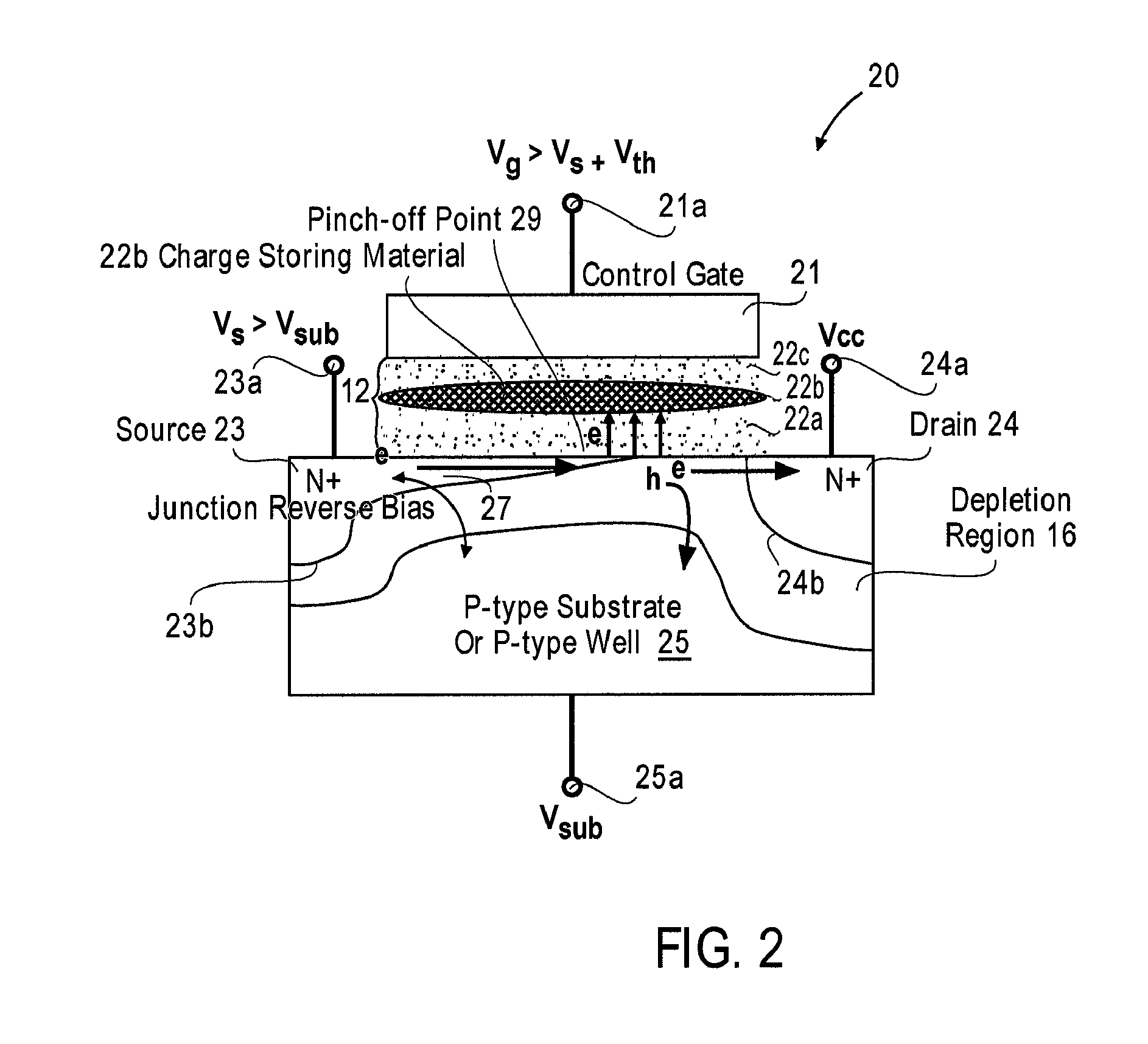
[0006]According to this invention, new HCI programming methods are provided to improve the programming efficiency, that is, to provide a higher injection rate toward the control gate 11 and into the storage material 12b with lower device current between source 13 and drain 14 to achieve the higher threshold voltage shifts of MOSFET device 10 with small programming current. In accordance with this invention, the highest current path of the device drain electrode is moved away from the high voltage path of charge pumping circuitry to the main voltage supply Vcc, which has more current capacity with a lower voltage drop from the external power source. Since only the main voltage supply Vcc is applied to the bitlines of an array of NVM cells (connected to the drain electrodes of a column of NVM cells), the ordinary logic circuitry to control the NVM array can be used for the selective bitline switching. The more complicated high voltage decoder with high voltage level shifters used in the prior art programming of the MOSFET 10 in an NVM cell is not required for switching the bitlines of an NVM array. This simplifies the bitline design in arrays of NVM cells. Due to smaller programming current and by shifting the current load to the main voltage supply Vcc, parallel programming is enabled for more NVM cells than in the prior art with improved programming uniformity in one programming cycle. Consequently, the disclosed programming method can lead to a very fast parallel programming operation in Non-Volatile Memory array devices.

Problems solved by technology

The programming efficiency is thus very low.
It becomes very challenging for charge pump circuit design to support a high current load while maintaining a constant higher drain 14 voltage bias during programming MOSFET 10 in an NVM cell.
For parallel programming an array of NVM cells, the programming uniformity can also be compromised from the high voltage supply dropout due to high current load.

Method used


Image

  • Method and structures for highly efficient hot carrier injection programming for non-volatile memories
  • Method and structures for highly efficient hot carrier injection programming for non-volatile memories
  • Method and structures for highly efficient hot carrier injection programming for non-volatile memories

Examples


Embodiment Construction

[0016]The present invention includes methods and structures to optimize the Hot Carrier Injection programming for NVM cells. Those of ordinary skill in the art will immediately realize that the embodiments of the present invention described herein are illustrative only and are not intended to be in any way limiting. Other embodiments of the present invention will readily suggest themselves to such skilled persons having the benefits of this disclosure.

[0017]In one aspect of this invention, an N-type Non-Volatile Memory (NVM) device 20 as shown in FIG. 2 includes N-type source 23 in an N+ region 23a and drain 24 in another N+ region 24a located in a P-type substrate or P-type Well 25. The control gate 21 is on top of but separated from the substrate 25 by thin dielectrics 22a and 22c and charge storing material 22b embedded in the thin dielectric 12. By applying a positive voltage to control gate terminal 21a an N-type channel region is formed between source 23 and drain 24 in the to...


PUM


Abstract

A method programs a memory cell by controlling a reverse bias voltage across the PN junction between a source electrode of a MOSFET in the memory cell and the substrate, and pulling back the pinch-off point of the inversion region toward the source electrode, thereby increasing the programming efficiency of the memory cell. The method applies the main positive supply voltage Vcc to, the drain electrode of the memory cell from the chip main voltage supply, rather than the conventional method of using a higher voltage than Vcc. To optimize the programming condition, the source voltage and the substrate voltage are adjusted to achieve the maximum threshold voltage shifts under the same applied gate voltage pulse condition (i.e. using the gate pulse with the same voltage amplitude and duration regardless of the source voltage and the substrate voltage). The substrate voltage to the drain voltage can not exceed the avalanche multiplication junction breakdown for a small programming current during the bias voltage adjustment.

Description

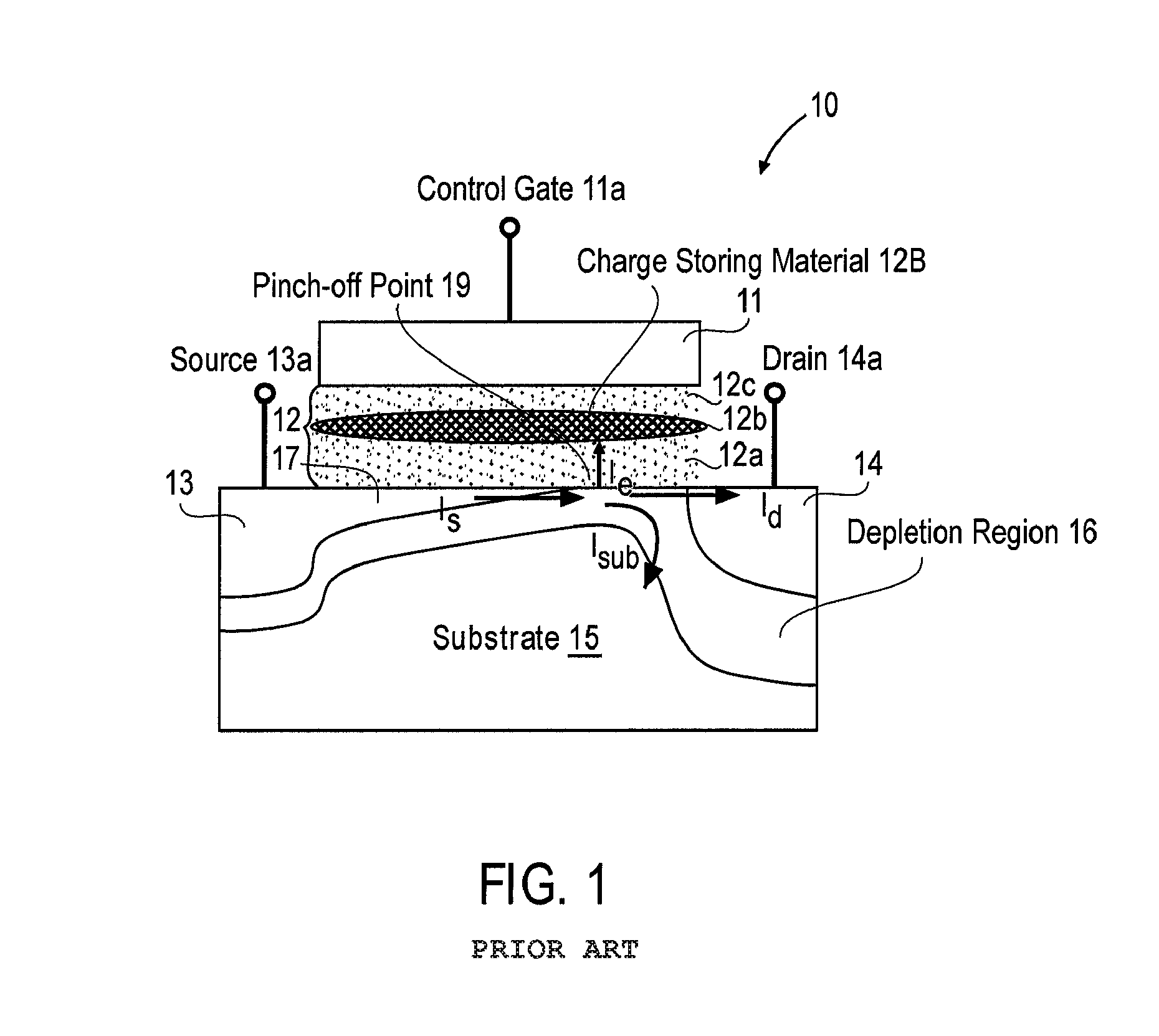
FIELD OF INVENTION[0001]This invention relates to methods and structures for programming Non-Volatile Memory (NVM) cells using highly efficient Hot Carrier Injection (HCI).BACKGROUND OF INVENTION[0002]As shown in FIG. 1, metal oxide semiconductor field effect transistor 10 (MOSFET) includes a source 13 and a drain 14 (connected respectively to source electrode 13a and drain electrode 14a) each with an impurity type opposite to the impurity type of the substrate 15. The source 13 and drain 14 are separated by a channel region in the substrate 15 underlying a control gate 11 formed over a dielectric layer 12 on top of the silicon substrate 15. When the voltage applied to the gate electrode 11a electrically connected to control gate 11 exceeds the threshold voltage of the MOSFET 10, the channel region in the substrate 15 between the source 13 and the drain 14 and just below the dielectric 12 under the control gate 11 of the MOSFET device 10 is inverted to the same conductivity type as ...

Claims


Application Information

Patent Timeline
Patent Type & Authority Patents(United States)
IPC IPC(8): G11C11/34
CPCG11C8/08G11C16/10G11C2216/10H01L29/7883
Inventor WANG, LEE
Owner PEGASUS SEMICON SHANGHAI CO LTD
Why Eureka
Try Eureka