Supercharge Your Innovation With Domain-Expert AI Agents!

Multi-component doping of copper seed layer

a technology of copper seed layer and multi-component doping, which is applied in the direction of electrolysis components, vacuum evaporation coatings, coatings, etc., can solve the problem of difficult sputtering geometry, insufficient barrier, and inability to form a metallic tantalum layer

Active Publication Date: 2010-07-06
APPLIED MATERIALS INC
View PDF15 Cites 3 Cited by
  • Summary
  • Abstract
  • Description
  • Claims
  • Application Information

AI Technical Summary

Benefits of technology

The patent describes a method of sputtering a copper seed layer with a mixture of reactive and non-reactive dopants. The reactive dopants, such as titanium, magnesium, and aluminum, help to alloy with copper, while the non-reactive dopants, such as palladium, tin, indium iridium, and silver, help to improve the electrical conductivity of the copper layer. The amount of each dopant can be determined through stress migration and electro migration testing. The resulting copper alloy has improved properties, such as higher conductivity and better resistance to corrosion. The patent also includes a copper sputtering target with a surface composed of this copper alloy.

Problems solved by technology

However, as the minimum feature width of advanced integrated circuits is being pushed to 0.13 μm and even lower, the aspect ratio of the via hole, that is, the ratio of its depth to its width, has increased to 5 and higher, a difficult geometry for sputtering.
However, the barrier thickness needs to be large enough to guarantee the barrier layer 22 is not formed with pin holes or localized areas that are so thin that they do not serve as an adequate barrier.
Furthermore, ALD is not readily usable to form a metallic tantalum layer, which has the advantage of bonding fairly well with the silicate dielectric.
We believe that these suggestions in the prior art are insufficient in determining a reasonable dopant contribution in copper seed layers grown in a commercial environment.

Method used


Image

  • Multi-component doping of copper seed layer
  • Multi-component doping of copper seed layer
  • Multi-component doping of copper seed layer

Examples


Embodiment Construction

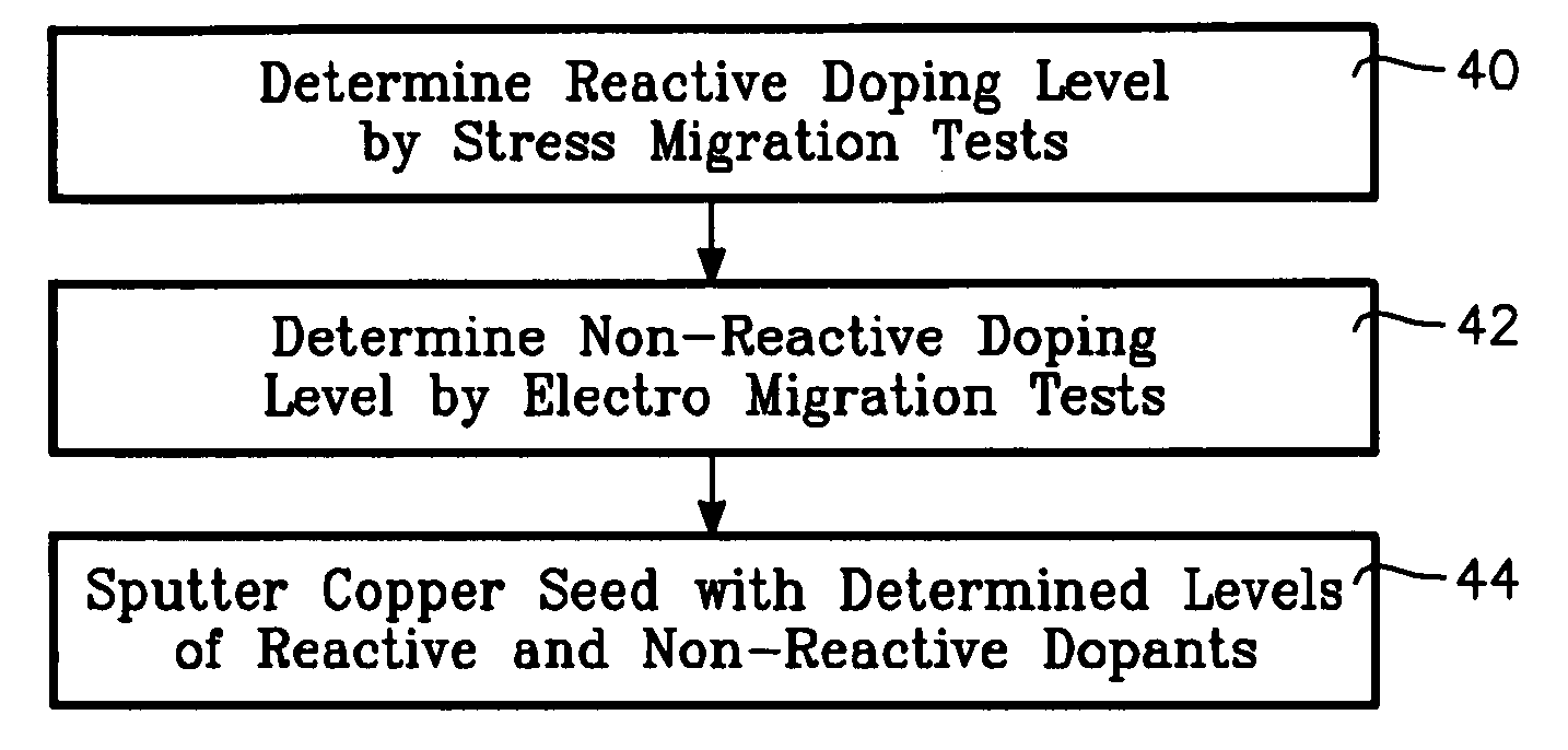
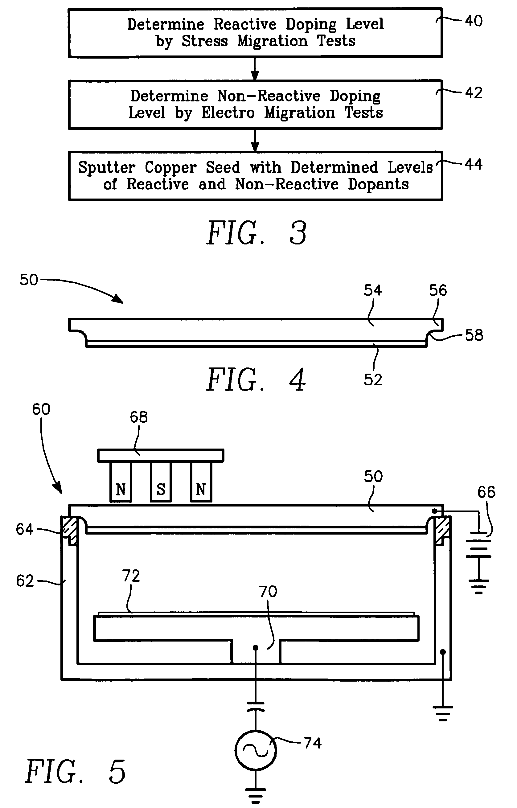
[0022]We believe that dopants for copper seed layer can be divided into two main classes, reactive and non-reactive, producing different effects.

[0023]Reactive dopants react with the copper and other metals to form a stable compound alloy similar to an intermetallic alloy. The surface of a such a copper alloy bonds well with the underlying barrier layers formed of other refractory metals such as tantalum, titanium, tungsten and their nitrides. That is, the copper alloy layer adheres well to the barrier layer.

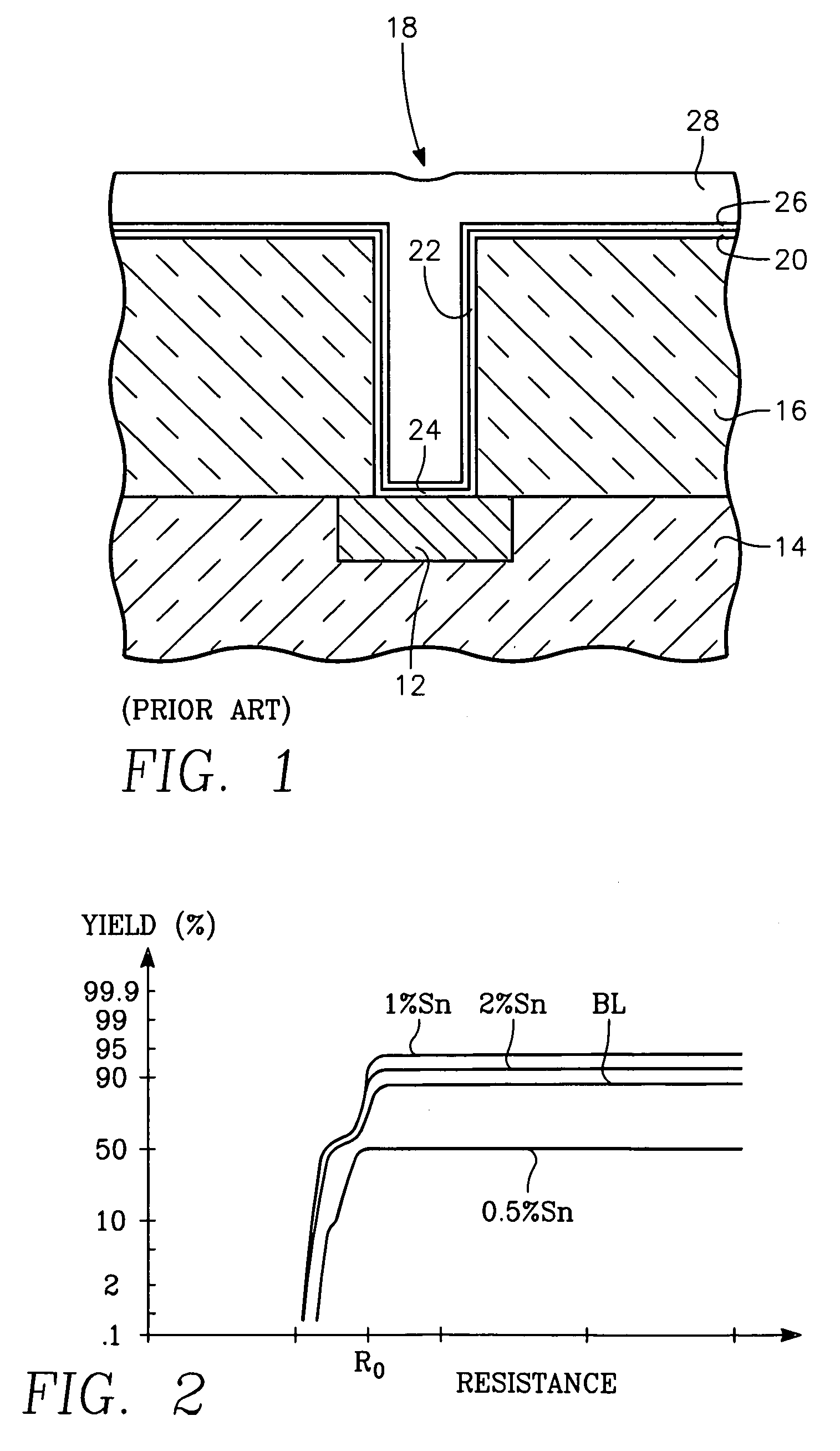
[0024]Horizontal electrical interconnections are formed in a multi-layer structure. In typical copper metallization, the copper line is deposited over a tantalum-based barrier layer, most usually a Ta / TaN bilayer with the metallic tantalum contacting the copper and the nitride contacting the oxide. The barrier layer in turn is deposited over an oxide dielectric layer, usually based on silicon oxide, perhaps including dopants such as fluorine. During fabrication and operation, th...


PUM

PropertyMeasurementUnit
thicknessaaaaaaaaaa
thicknessaaaaaaaaaa
concentrationaaaaaaaaaa

Abstract

A method of sputtering a copper seed layer and the target used therewith. The copper included in the sputtering target includes a first dopant reactive with copper and a second dopant unreactive with copper. Examples of the first dopant include Ti, Mg, and Al. Examples of the second dopant include Pd, Sn, In, Ir, and Ag. The amount of the first dopant may be determined by testing stress migration and that of the second dopant by testing electromigration.

Description

FIELD OF THE INVENTION[0001]The invention relates generally to sputtering of materials. In particular, the invention relates to a copper seed layer in a via structure.BACKGROUND ART[0002]Copper is replacing aluminum as the favored metallization for forming advanced integrated circuits. The copper is used not only for the horizontal wiring patterns in multiple wiring levels but also for the vertical connections between wiring levels. An inter-level via structure is illustrated in the cross-sectional view of FIG. 1. A conductive feature 12, typically of copper, is formed in the surface of a lower level dielectric layer 14, typically of silica or other silicate glass although low-k dielectrics of differing compositions have been proposed. An upper level dielectric layer 16 is deposited over the lower-level dielectric layer 14 and its included conductive feature 12. The dielectric layer 16 typically has a thickness of about 1 μm, and it is not anticipated that the thickness can be reduc...

Claims


Application Information

Patent Timeline
Patent Type & Authority Patents(United States)
IPC IPC(8): C23C14/34
CPCC23C14/046C23C14/165C23C14/3414
Inventor CHEN, JIEDING, PEIJUNRENGARAJAN, SURAJCHEN, LINGVO, TRAM
Owner APPLIED MATERIALS INC
Features
  • R&D
  • Intellectual Property
  • Life Sciences
  • Materials
  • Tech Scout
  • Unparalleled Data Quality
  • Higher Quality Content
  • 60% Fewer Hallucinations
Learn More