

Bottom electrode mask design for ultra-thin interlayer dielectric approach in MRAM device fabrication
a technology of mram device and bottom electrode, applied in the field of bottom electrode mask layout, can solve the problems of major obstacles, lack of high etch selectivity between be films and ild films, and the chance of device failure is increased, so as to improve the planarization of be ild, reduce the delamination of the etch stop ild, and improve the effect of etching uniformity across the wafer
- Summary
- Abstract
- Description
- Claims
- Application Information
AI Technical Summary
Benefits of technology
Problems solved by technology
Method used
Image

Examples
Embodiment Construction
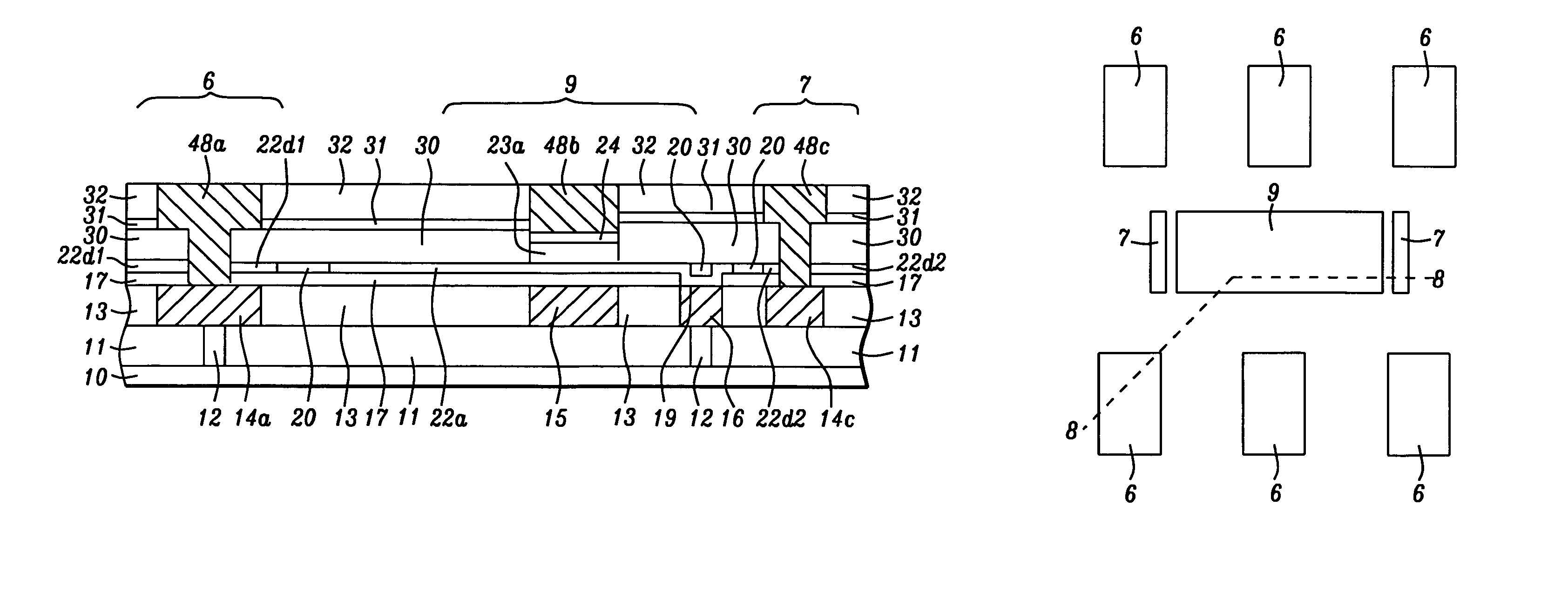
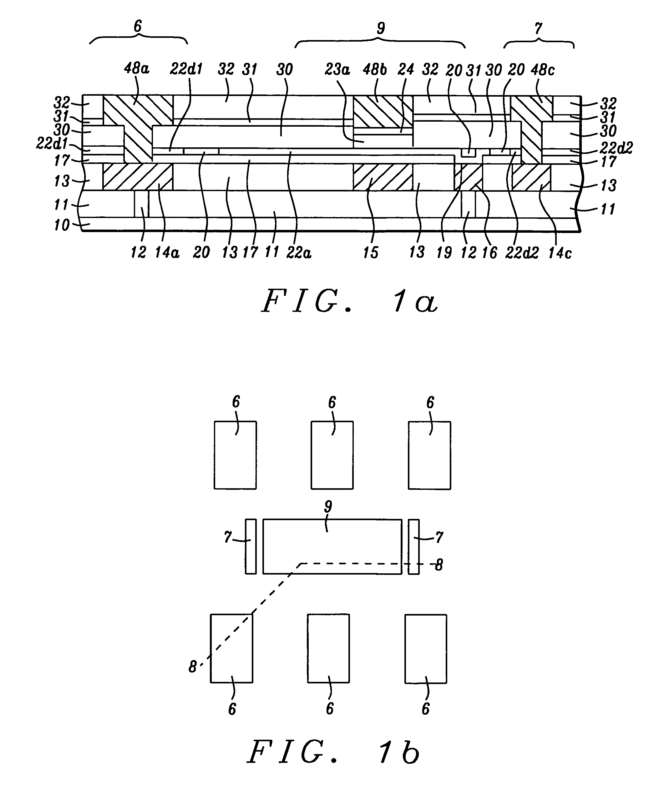
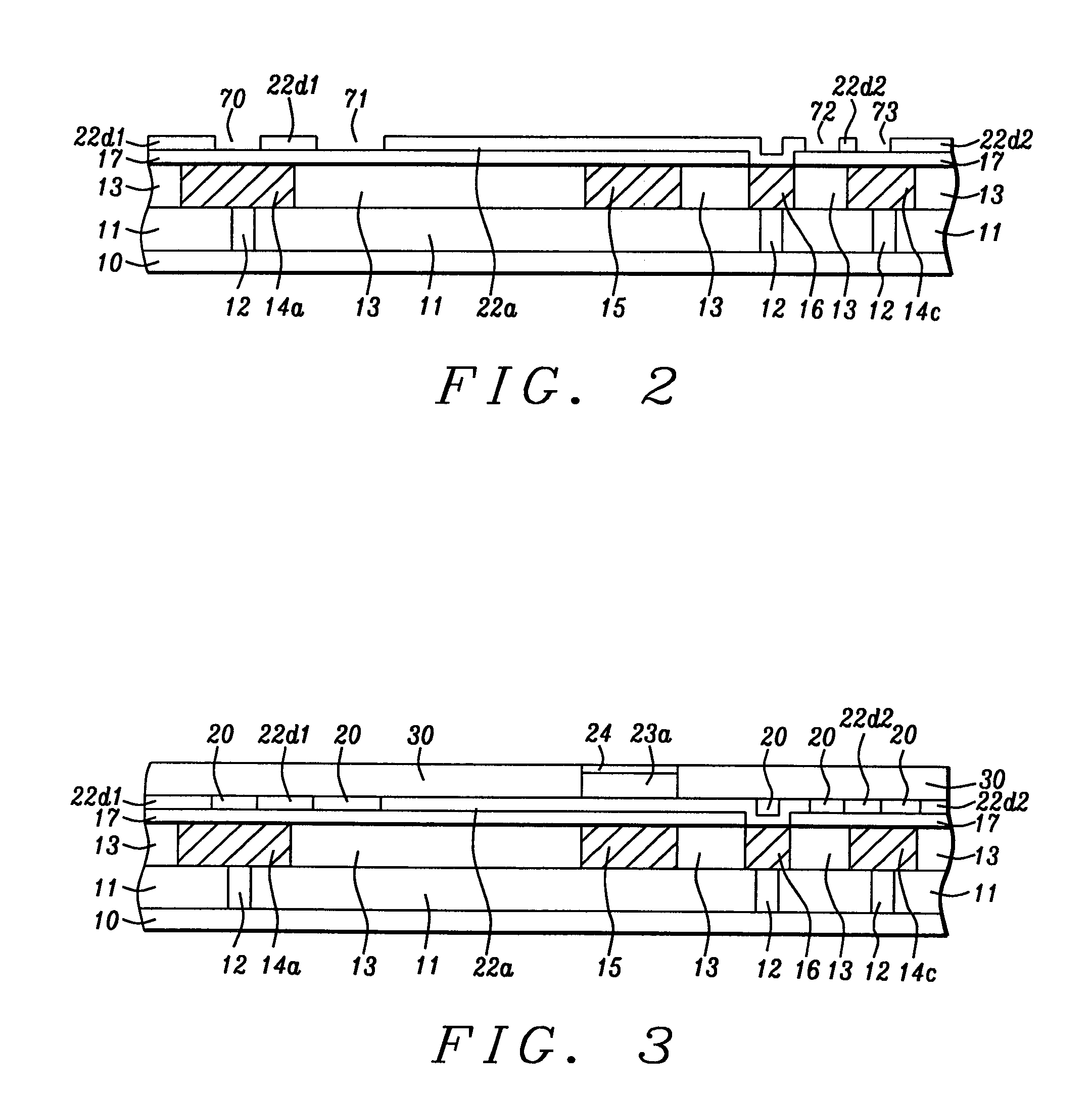
[0032]The present invention is a novel BE layout (mask) used to pattern a BE layer formed in a MRAM device. The present invention also encompasses a MRAM structure and a method for forming the same that minimizes delamination of interlevel dielectric (ILD) layers formed between a word line (WL) layer and a bit line (BIT) layer, improves ILD layer thickness uniformity, and reduces pinholes in an etch stop ILD layer that can lead to WL corrosion. Although the exemplary embodiment depicts a MRAM device with a 1T1MTJ architecture, the present invention may also apply to other magnetic memory devices known in the art that include a BE layer and an array of MTJ devices. Drawings are provided by way of example and are not intended to limit the scope of the invention. The MTJ devices may have a top spin valve, bottom spin valve, or multi-layer spin valve configuration as appreciated by those skilled in the art. Two layers are said to be coplanar when a top surface of each layer lies in the ...
PUM
 Abstract
Description
Claims
Application Information