TSVS having chemically exposed TSV tips for integrated circuit devices

a technology of integrated circuits and tsv tips, which is applied in the direction of semiconductor devices, semiconductor/solid-state device details, electrical apparatus, etc., can solve the problems of reducing the reliability of ic, reducing the lifetime of minority carriers, and reducing the separation distance between the exposed electrical conductive filler material of the tsv tip and the substra

Active Publication Date: 2010-11-16
TEXAS INSTR INC
View PDF26 Cites 23 Cited by
  • Summary
  • Abstract
  • Description
  • Claims
  • Application Information

AI Technical Summary

Benefits of technology

[0007]The Present Inventors have recognized that for a conventional via-first TSV process, the TSV tips get damaged, scratched and / or cracked since the last portion of the backgrind process grinds the TSV tips. Even with a conventional CMP and / or a chemical etch step following backgrinding, damage, scratching and / or cracking generally still remains in the dielectric liner, the diffusion barrier metal (if present) and the electrically conductive filler material of the TSVs. As a result of such residual damage, scratching, cracking and the resulting leakage paths, the separation distance between the exposed electrical conductive filler material of the TSV tip and the substrate (e.g., Si) can be too small to prevent significant electrical leakage between the TSV and the surrounding substrate (i.e. when the TSV and the substrate are tied to different voltage levels). Such leakage can be at a high enough level to significantly reduce IC performance and / or circuit yield, particularly for certain RF devices (e.g., RF power amplifier), and can also lead to degraded reliability of the IC.
[0008]Moreover, the Present Inventors have recognized that conventional backgrinding into the TSV tips smears the electrically conductive filler material (e.g., metal) onto the back surface of the substrate. Such contamination can significantly reduce minority carrier lifetimes in the active circuitry.
[0009]The Present Inventors have discovered by modifying the conventional backgrinding process so that the backgrinding process only provides a portion of the wafer thinning, with chemically etching provided the final portion of the wafer thinning, damage, scratching or cracking damage to the dielectric liner, the diffusion barrier metal (if present) and the electrically conductive filler material of the TSV can be significantly reduced or eliminated. As a result, electrical isolation between the TSVs and the substrate can be significantly improved by embodiments of the invention.
[0010]Backgrinding, according to embodiments of the invention, thus approaches but does not reach the embedded TSV tips and accordingly leaves a residual protective substrate layer portion, thus avoiding direct physical contact of the TSV tip with the abrasive surface of the backgrinding tool. As described above, avoiding direct physical contact of the TSV tip with the backgrind tool has been found by the Present Inventors to avoid, or at least significantly reduce, mechanical damage to the electrically conductive filler material, diffusion barrier metal (if present) and dielectric liner surrounding the TSV, as well as reduce or eliminate smearing of the electrically conductive filler material (e.g., metal) on the bottom substrate surface. As defined herein, a “chemical etch” refers to a wet or dry (e.g., plasma) etch that is exclusive of mechanical etching. A “chemical etch exclusive of mechanical etching” as used herein can include CMP provided the CMP process is configured to function as a chemical etch by providing a selectivity between the material of the wafer (e.g., silicon) and the dielectric liner of >10:1, and thus have at most a minimal mechanical component. For example, a CMP process having no abrasive particles (e.g., no particles having a Mohs hardness≧the Mohs hardness of silica) can in certain arrangements provide a minimal mechanical component.
[0011]Embodiments of the invention generally comprise backgrinding for partial substrate thinning to leave a protective substrate layer to retain the embedded TSV tip, followed by a sequence of chemical etches for removing the protective substrate layer and a portion of the dielectric liner to expose the electrically conductive filler material of the TSV tip. Integral TSV tips are formed that generally protrude from the bottom surface of the substrate, and are referred to herein as protruding integral TSV tips. Leaving a protective substrate portion after backgrinding has been found generally to significantly improve electrical isolation and thus reduce leakage between TSV tip and the surrounding substrate.

Problems solved by technology

As a result of such residual damage, scratching, cracking and the resulting leakage paths, the separation distance between the exposed electrical conductive filler material of the TSV tip and the substrate (e.g., Si) can be too small to prevent significant electrical leakage between the TSV and the surrounding substrate (i.e. when the TSV and the substrate are tied to different voltage levels).
Such leakage can be at a high enough level to significantly reduce IC performance and / or circuit yield, particularly for certain RF devices (e.g., RF power amplifier), and can also lead to degraded reliability of the IC.
Such contamination can significantly reduce minority carrier lifetimes in the active circuitry.
Thicker values for the protective layer (t1) can still generally be used with embodiments of the invention, but may lead to higher fabrication cost for the subsequent etch steps.
Such variation can degrade the controllability of the process.
Lower selectivity can cause excessive loss of the electrically conductive filler material 114.
The tape protects the TSV tips, but can lead to certain process challenges associated with adhesive residue after pick and place, such as voids between the tape adhesive and the wafer surface with the TSV tips because of the tall height of the TSV tips relative to the adhesive thickness.

Method used


Image

  • TSVS having chemically exposed TSV tips for integrated circuit devices
  • TSVS having chemically exposed TSV tips for integrated circuit devices
  • TSVS having chemically exposed TSV tips for integrated circuit devices

Examples


examples

[0056]Embodiments of the present invention are further illustrated by the following specific Examples, which should not be construed as limiting the scope or content of embodiments of the invention in any way.

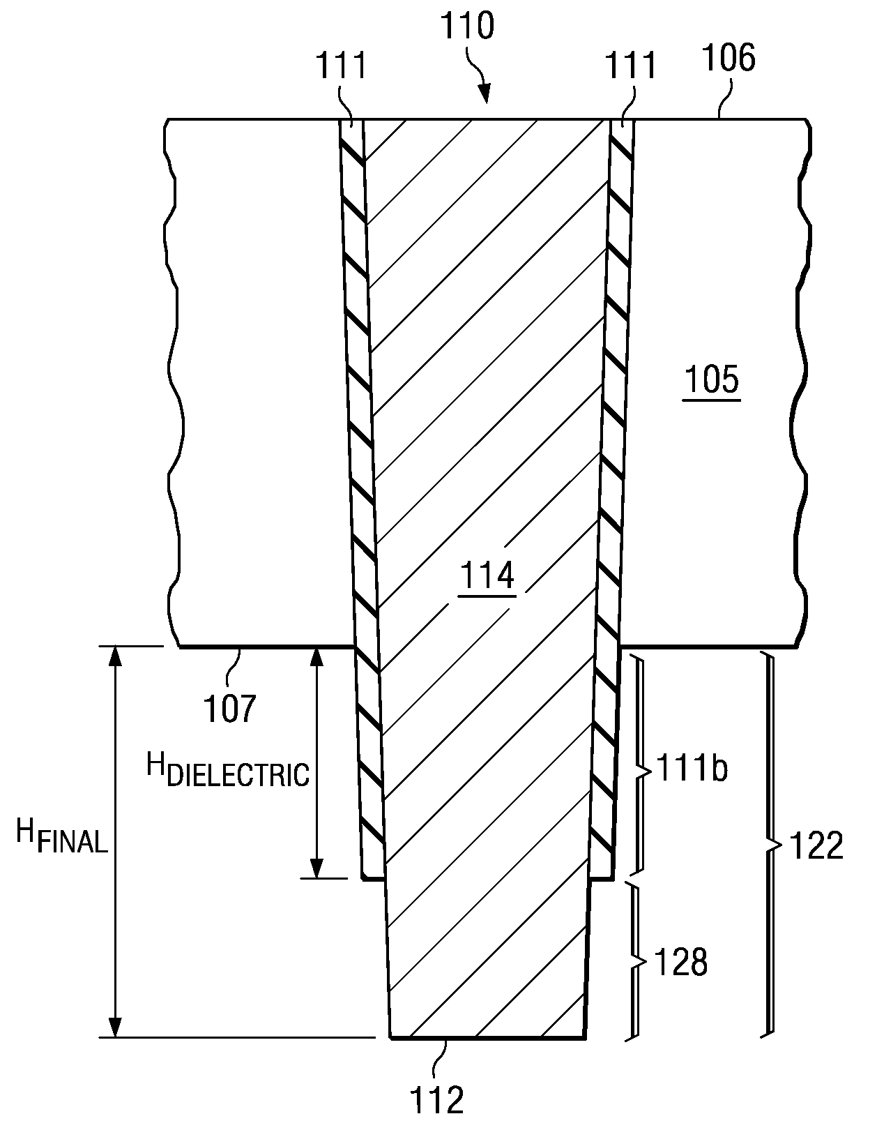
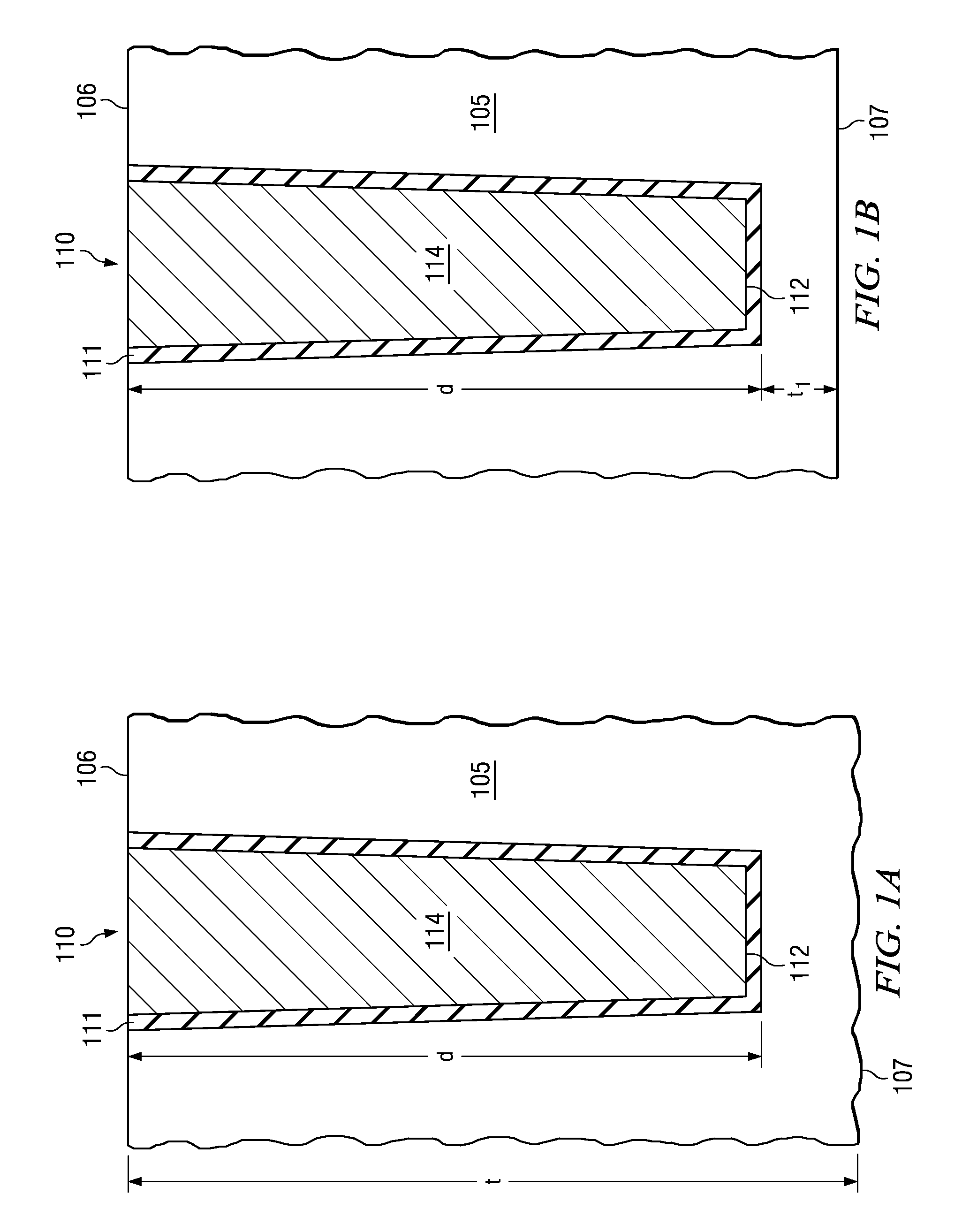
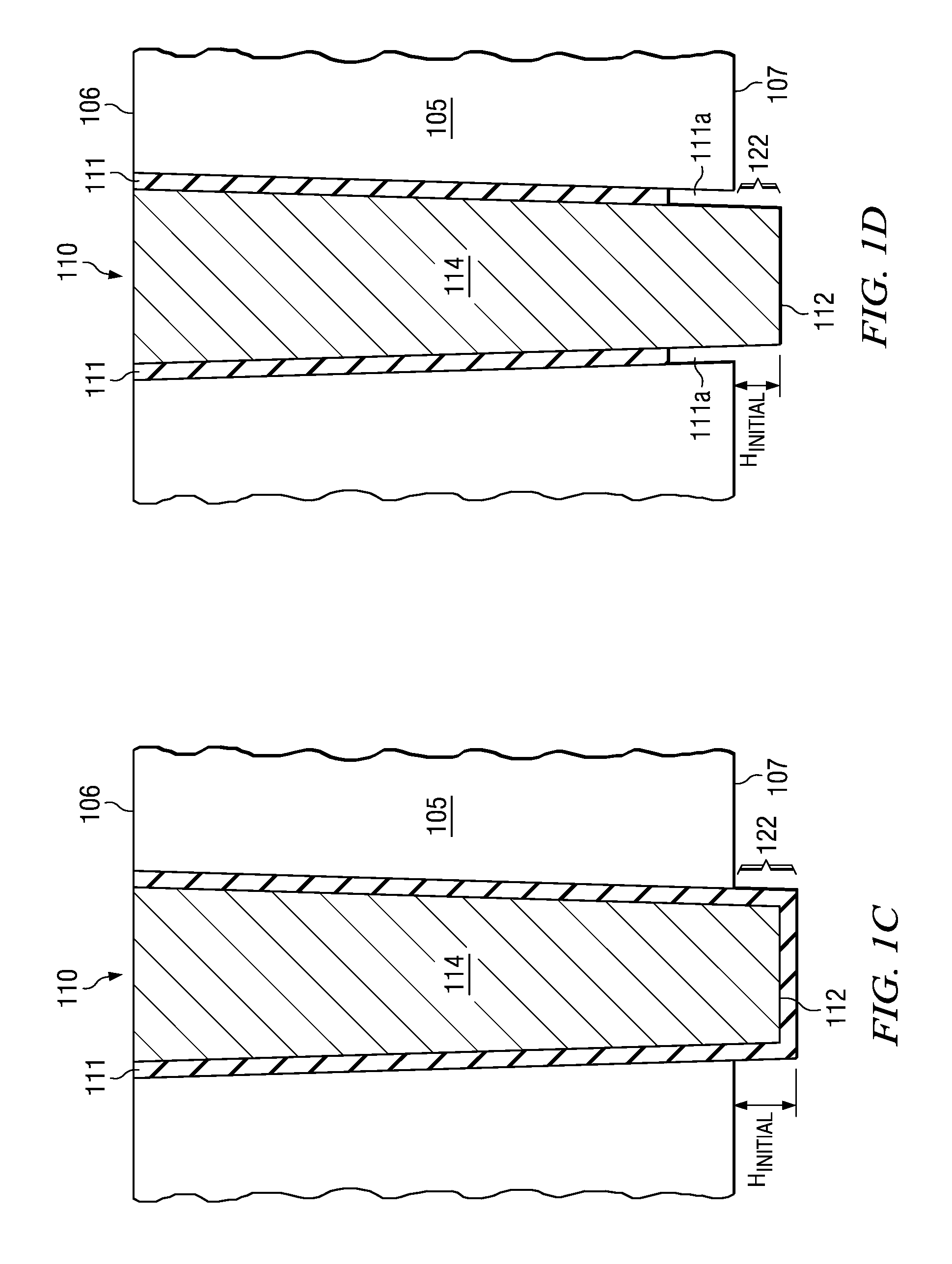
[0057]Bulk silicon wafers were fabricated to include a plurality of embedded TSVs that were approximately 130 μm deep, filled with copper, and lined with a SiO2 liner and a TaN barrier. The TSVs had a diameter from 20 to 30 μm and a pitch of 50 to 70 μm. The wafer thinning and die attach flow is described below. The active circuit face of the wafer was bonded to a reusable Si carrier wafer using an adhesive. Backgrind was used to obtain a wafer thickness of about 137 μm followed by polishing to remove about 2 μm more of the substrate to result in a wafer thickness of 135+ / −3 μm. The TSVs thus remained embedded after the backgrinding and polishing processing and the thickness of the protective substrate layer was about 5 μm.

[0058]The first backside etch was a silicon etch for et...


PUM

PropertyMeasurementUnit
thicknessaaaaaaaaaa
heightaaaaaaaaaa
heightaaaaaaaaaa

Abstract

A method for fabricating ICs including via-first through substrate vias (TSVs) and ICs and electronic assemblies therefrom. A substrate having a substrate thickness including a top semiconductor surface and a bottom surface is provided including at least one embedded TSV including a dielectric liner and an electrically conductive filler material formed on the dielectric liner. A portion of the bottom surface of the substrate is mechanically removed to approach but not reach the embedded TSV tip. A protective substrate layer having a protective layer thickness remains over the tip of the embedded TSV after the mechanical removing. Chemical etching exclusive of mechanical etching for removing the protective substrate layer is used form an integral TSV tip that has an exposed tip portion that generally protrudes from the bottom surface of the substrate. The chemical etching is generally a three step chemical etch.

Description

CROSS REFERENCE TO RELATED APPLICATIONS[0001]This application claims the benefit of Provisional Application Ser. No. 61 / 052,487 entitled “ETCH METHOD FOR PREPARING THE TIPS OF THROUGH-SILICON-VIAS TO ENABLE DIE OR WAFER LEVEL ATTACH TO ANOTHER DIE OR WAFER”, filed May 12, 2008, which is herein incorporated by reference in its entirety.FIELD OF THE INVENTION[0002]Embodiments of the present invention relate to integrated circuits (IC) devices having through substrate vias.BACKGROUND[0003]As known in the art, through-substrate vias (referred to herein as TSVs), which are commonly referred to as through-silicon vias, are vertical electrical connections that extend from one of the electrically conductive levels formed on the top surface of a wafer or IC die (e.g., contact level or one of the metal interconnect levels) to the backside (bottom) surface. As a result, the TSV comprising device can be bonded face-up and utilize vertical electrical paths to couple to other IC devices (e.g., on...

Claims


Application Information

Patent Timeline
Patent Type & Authority Patents(United States)
IPC IPC(8): H01L21/44
CPCH01L21/76898H01L23/481H01L2924/0002H01L2924/00
Inventor BONIFIELD, THOMAS D.GOODLIN, BRIAN E.EISSA, MONA M.
Owner TEXAS INSTR INC
Why Eureka
Try Eureka