Glass-based SOI structures

a glass-based, soi technology, applied in the direction of semiconductor devices, electrical equipment, transistors, etc., can solve the problems of difficult replacement of silicon wafers with glass or glass-ceramic of the type, quartz itself is a relatively expensive material, and the cost of such structures has been the cost of silicon wafers, etc., to achieve strong bonding and higher pressur

Inactive Publication Date: 2010-11-23
CORNING INC
View PDF48 Cites 23 Cited by
  • Summary
  • Abstract
  • Description
  • Claims
  • Application Information

AI Technical Summary

Benefits of technology

[0194]Because the invention uses low to moderate temperatures, pressures, electric field strengths, and vacuum levels, the requirements which the processing chamber needs to satisfy are not demanding, which is another important advantage of the invention, i.e., the invention can be practiced with equipment which is both relatively inexpensive and widely available or easily fabricated for custom applications.
[0195]FIG. 1C shows the central step of the process, i.e., step (C), where the first and second substrates are bonded to one another. Step (C) is performed for a period of time sufficient for the first and second substrates to bond to one another at the first and second bonding surfaces. For example, step (C) can be performed for a period between 45 and 90 minutes. Shorter periods of time are, of course, generally preferred (e.g., times less than 30 minutes) and in a commercial setting, it is expected that the time required to perform step (C) can be reduced to a period of 5-15 minutes or less through the optimization of substrate materials, processing temperatures, and applied voltages.
[0196]Step (C) is preferably performed under moderate vacuum conditions, i.e., chamber 40 is evacuated while step (C) is performed. Preferably, the pressure in the chamber is less than or equal to 1 millibar, and most preferably, less than or equal to 10−3 millibars. Alternatively, step (C) can be performed in an inert atmosphere, such as, an atmosphere of argon, helium, or the like.
[0197]As discussed above and shown in FIG. 1C, step (C) is performed with V1>V2 and preferably with T1<T2, where V1 and T1 are, respectively, the voltage and temperature at force-applying surface 12, and V2 and T2 are, respectively, the voltage and temperature at force-applying surface 22. In the examples described below, the second substrate was located below the first substrate as shown in FIG. 1C, although the opposite orientation can be used if desired. Also, vertical or other orientations for the substrates can be used, if desired.
[0198]V1 and V2 preferably satisfy the relationship:100 volts / cm≦(V1−V2) / D≦40 kilovolts / cm,where D is the distance between the first and second force-applying surfaces during step (C). A preferred value for the (V1−V2) / D ratio ranges between about 5-20 KV / cm.
[0199]T1 and T2 preferably satisfy the relationships:TS−350≦T1≦TS+350; andTS−350≦T2≦TS+350;where TS is the strain point of the oxide glass or oxide glass-ceramic and TS, T1, and T2 are in degrees centigrade. As discussed above, TS is less than 1000° C., can be less than 800° C., and may also be less than about 700° C.

Problems solved by technology

To date, a major part of the cost of such structures has been the cost of the silicon wafer which supports the oxide layer, topped by the Si thin film, i.e., a major part of the cost has been the support substrate.
Although the use of quartz as a support substrate has been mentioned in various patents (see U.S. Pat. Nos. 6,140,209 6,211,041, 6,309,950, 6,323,108, 6,335,231, and 6,391,740), quartz is itself a relatively expensive material.
In particular, it is difficult to replace a silicon wafer with a glass or glass-ceramic of the type which can be manufactured in large quantities at low cost, i.e., it is difficult to make cost effective SOG structures.

Method used


Image

  • Glass-based SOI structures
  • Glass-based SOI structures
  • Glass-based SOI structures

Examples


example 1

[0248]A 4-inch diameter phosphorus-doped silicon wafer (hereinafter referred to as the “silicon wafer”) having a thickness of 0.525 mm was implanted with hydrogen ions at 69 KeV at a concentration of 6×10¹⁶ ions / cm2 using commercially available, room temperature, ion implantation techniques. The phosphorus-doped silicon had a 0° C. CTE of 24×10−7 / ° C. and a 300° C. CTE of 38×10−7 / ° C. The wafer was obtained from SiliconSense Inc., Nashua, N.H., and, as reported by the manufacturer, had a resistivity of 1-10 ohm cm. Boron-doped silicon wafers were also used in various of the examples with equivalent results to the phosphorus-doped wafers.

[0249]A 4-inch diameter glass wafer having a thickness of 1 mm was washed in detergent, rinsed in distilled water, soaked in 10% nitric acid for 1 hour, and finally rinsed again in distilled water. It was then placed in a clean room hood and allowed to dry.

[0250]The glass wafer was made of CORNING INCORPORATED GLASS COMPOSITION NO. 7070. On a weight ...

example 2

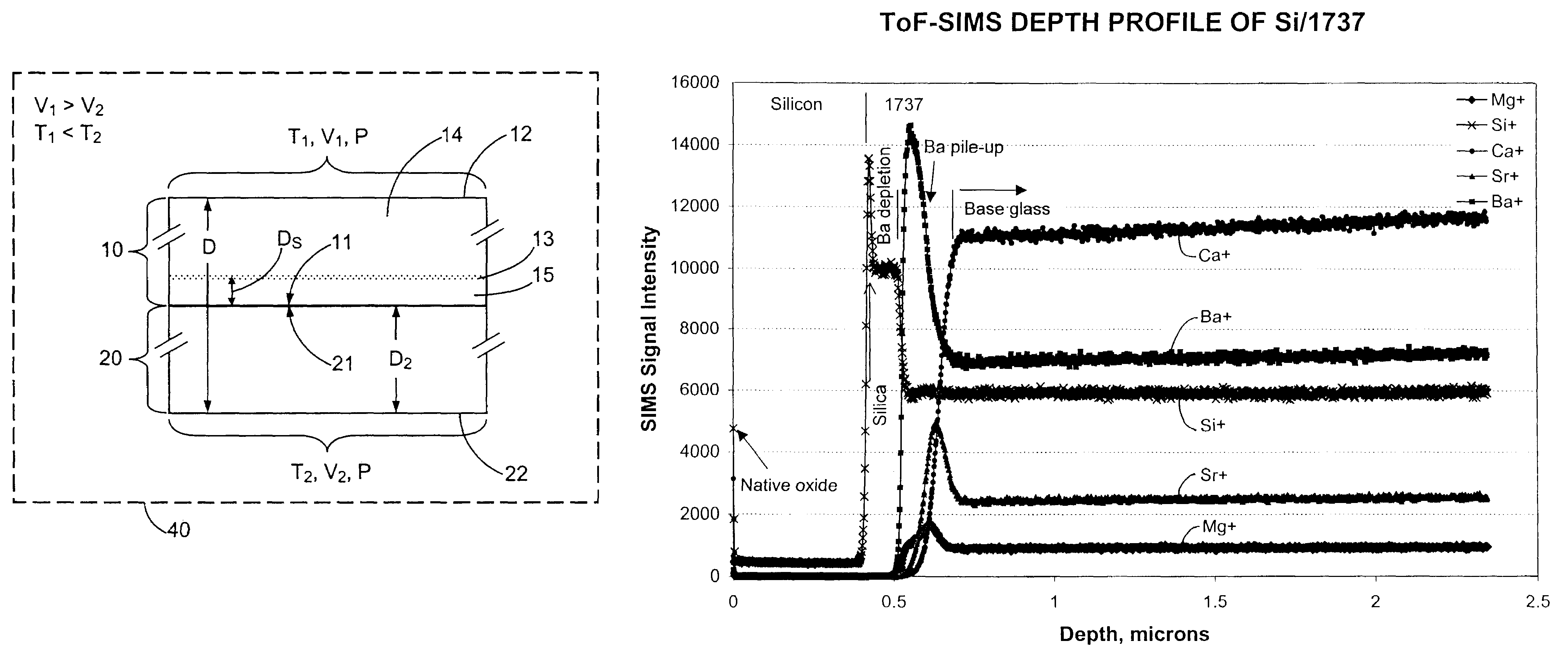
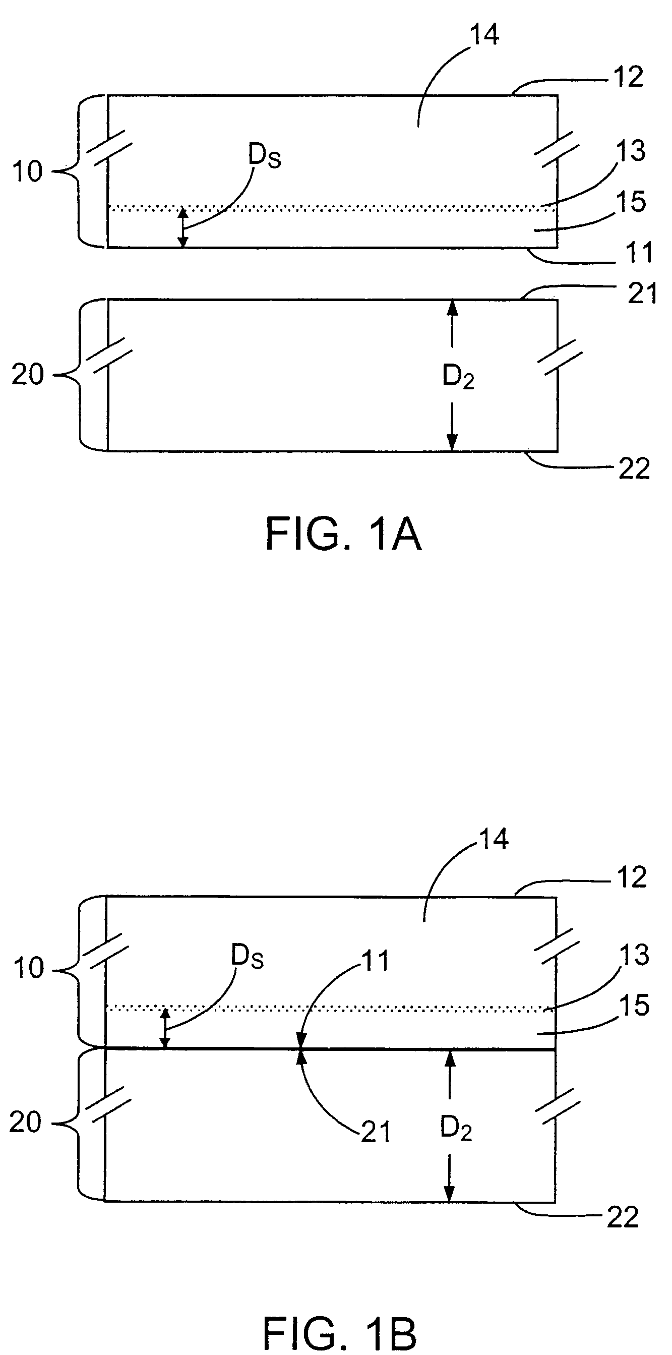
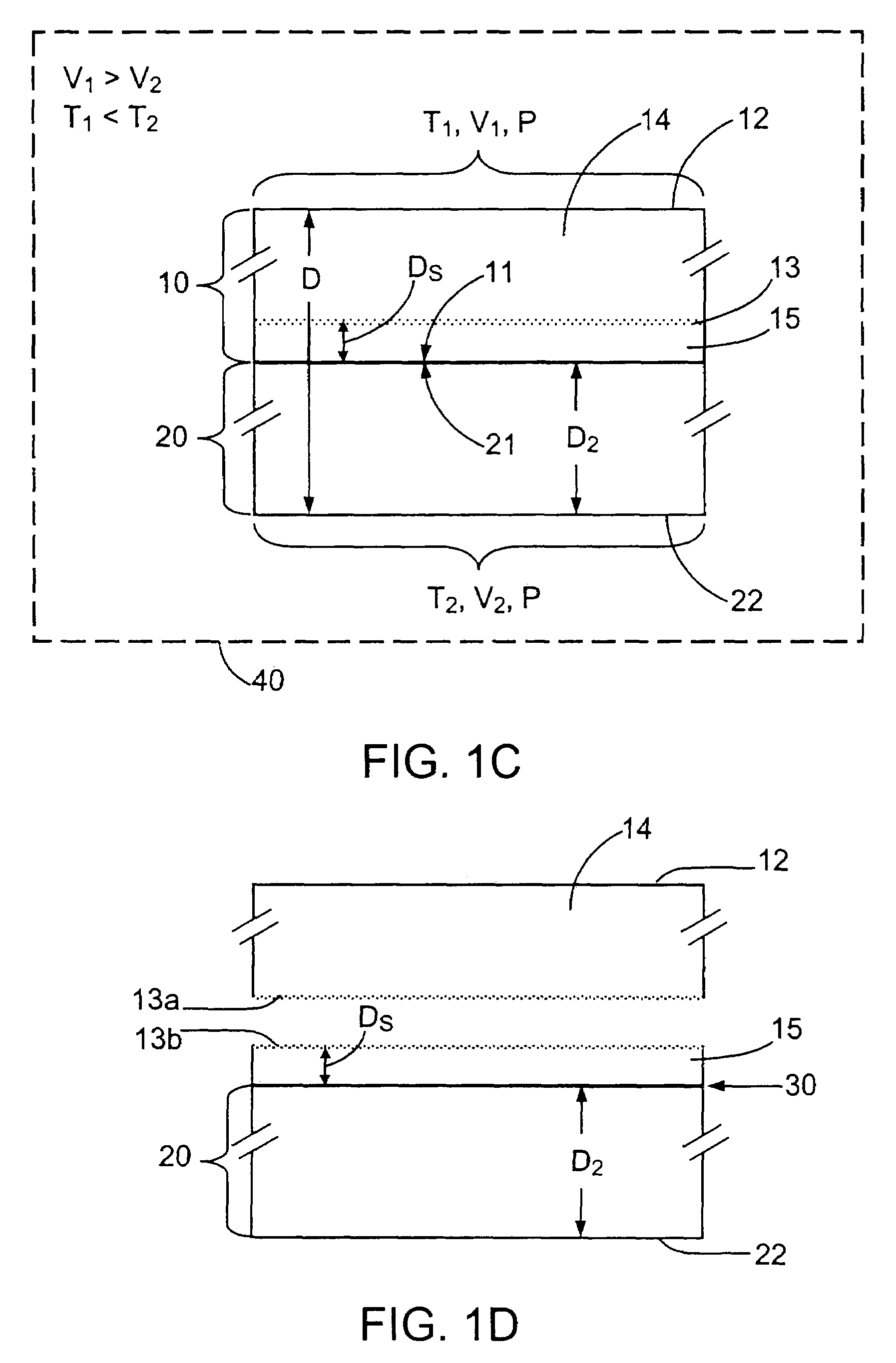
[0256]The experiment of Example 1 was repeated except that the two wafers, glass and silicon, were held at 450° C. and 400° C. respectively. This was done to take advantage of the thermal stress generated by the thermal differential to separate the thin silicon film from the silicon wafer after cooling. The differential heating was achieved by selecting the temperatures of the force-applying plungers of the bonder. The 450° C. and 400° C. values represent the temperatures of the plungers and thus the temperatures at the bottom surface of the glass wafer and the top surface of the silicon wafer, respectively, i.e., the temperatures at surfaces 22 and 12 in FIG. 1C

[0257]In this case, the glass wafer with a 0.4-micron layer of silicon (an SOI configuration) and the remainder of the Si wafer were easily separated, and thus an SOI glass wafer was successfully obtained. This result indicates that the thermal stress generated by a thermal differential is necessary in generating a glass-bas...

example 3

[0259]In this example, the Si wafer was first etched with a pattern of circular islands separated from one another. The islands were about 150 microns in diameter. This patterned wafer was ion implanted and then the process of Example 2 was used to transfer a Si layer about 0.4 microns thick onto the glass wafer. An SOI structure with an excellent bond between the Si layer and glass wafer was created in this case.

[0260]This island technique is expected to be of particular value when making large wafers where a thermal expansion mismatch between the glass and the Si is most likely to lead to delamination or other damage to the SOI structure.

[0261]The pattern etched or otherwise formed in the silicon wafer may be any geometric pattern which produces isolated islands of silicon. The size and the distance between the islands can be adjusted according to the requirements. If desired, a thin layer of silicon may be deposited via standard techniques to establish connectivity between all or...


PUM


Abstract

Semiconductor-on-insulator (SOI) structures, including large area SOI structures, are provided which have one or more regions composed of a layer (15) of a substantially single-crystal semiconductor (e.g., doped silicon) attached to a support substrate (20) composed of an oxide glass or an oxide glass-ceramic. The oxide glass or oxide glass-ceramic is preferably transparent and preferably has a strain point of less than 1000° C., a resistivity at 250° C. that is less than or equal to 1016 Ω-cm, and contains positive ions (e.g., alkali or alkaline-earth ions) which can move within the glass or glass-ceramic in response to an electric field at elevated temperatures (e.g., 300-1000° C.). The bond strength between the semiconductor layer (15) and the support substrate (20) is preferably at least 8 joules / meter2. The semiconductor layer (15) can include a hybrid region (16) in which the semiconductor material has reacted with oxygen ions originating from the glass or glass-ceramic. The support substrate (20) preferably includes a depletion region (23) which has a reduced concentration of the mobile positive ions.

Description

CROSS-REFERENCE TO RELATED APPLICATION[0001]This present application is a divisional under 35 US.C. §121 of Ser. No. 11 / 650,270, filed on Jan. 5, 2007, now U.S. Pat. No. 7,476,940; which is a divisional under 35 US.C. §121 of Ser. No. 10 / 799,582 filed on Feb. 12, 2004, now U.S. Pat. No. 7,176,528; which in turn claims the benefit of U.S. Provisional Application No. 60 / 448,176 filed on Feb. 18, 2003, which is hereby incorporated herein by reference. The Applicant claims the benefit of priority under 35 US.C. §120 & 121 of the above-identified applications.FIELD OF THE INVENTION[0002]This invention relates to semiconductor-on-insulator (SOI) structures. More particularly, the invention relates to 1) methods for making such structures and 2) novel forms of such structures.[0003]To date, the semiconductor material most commonly used in semiconductor-on-insulator structures has been silicon. Such structures have been referred to in the literature as silicon-on-insulator structures and th...

Claims


Application Information

Patent Timeline
Patent Type & Authority Patents(United States)
IPC IPC(8): H01L29/786H01L21/20H01L21/30H01L21/46H01L21/762
CPCH01L21/76254H01L21/2007H01L21/20
Inventor COUILLARD, JAMES G.GADKAREE, KISHOR P.MACH, JOSEPH F.
Owner CORNING INC
Why Eureka
Try Eureka