Method of depositing thin film and method of manufacturing semiconductor using the same

a technology of thin film and anti-reflective film, which is applied in the direction of semiconductor devices, instruments, photomechanical treatment, etc., can solve the problems of nitrided-oxide film suffering, delay in actual application of amorphous organic carbon anti-reflective film, and increase the difficulty encountered in semiconductor manufacturing process. , to achieve the effect of increasing etching resistance, low extinction coefficient and high selectivity

Active Publication Date: 2010-11-30
WONIK IPS CO LTD
View PDF10 Cites 9 Cited by
  • Summary
  • Abstract
  • Description
  • Claims
  • Application Information

AI Technical Summary

Benefits of technology

[0009]Accordingly, the present invention has been made keeping in mind the above problems occurring in the prior art, and an object of the present invention is to provide a method of manufacturing a semiconductor, suitable for the formation of an amorphous carbon anti-reflective film having high selectivity by increasing etching resistance while maintaining a low extinction coefficient.
[0010]Another object of the present invention is to provide an apparatus for manufacturing a semiconductor, suitable for the formation of an amorphous carbon anti-reflective film having high selectivity by increasing etching resistance while maintaining a low extinction coefficient.
[0012]In addition, the present invention provides a method of manufacturing a semiconductor, suitable for the formation of an amorphous carbon anti-reflective film on a semiconductor substrate, the method comprising (a) depositing an amorphous organic carbon film on the bottom film of the semiconductor substrate; and (b) applying RF power, together with either MF power or DC power, to the substrate having the amorphous organic carbon film deposited thereon for ionization and deposition of a carbon source gas, to form a large amount of plasma ions, and applying the plasma ions to a wafer to cause an ion impact effect, thus increasing the density of the film, resulting in increased compressive stress.

Problems solved by technology

Since the degree of integration of almost all highly integrated semiconductor devices having high capacities, such as DRAMs or FRAMs, is doubled every year, the degree of difficulty encountered in semiconductor manufacturing processes is further increasing.
However, the nitrided-oxide film suffers because it causes defects and entails complicated processes.
As in FIG. 1, when the deposition temperature is increased, it is not easy to increase hardness and an extinction coefficient (k) associated with anti-reflectivity, due to the expanded graphite structure, therefore resulting in delayed actual application of the amorphous organic carbon anti-reflective film to a semiconductor process.

Method used


Image

  • Method of depositing thin film and method of manufacturing semiconductor using the same
  • Method of depositing thin film and method of manufacturing semiconductor using the same
  • Method of depositing thin film and method of manufacturing semiconductor using the same

Examples


Embodiment Construction

[0021]Hereinafter, a detailed description will be given of the present invention, with reference to the appended drawings.

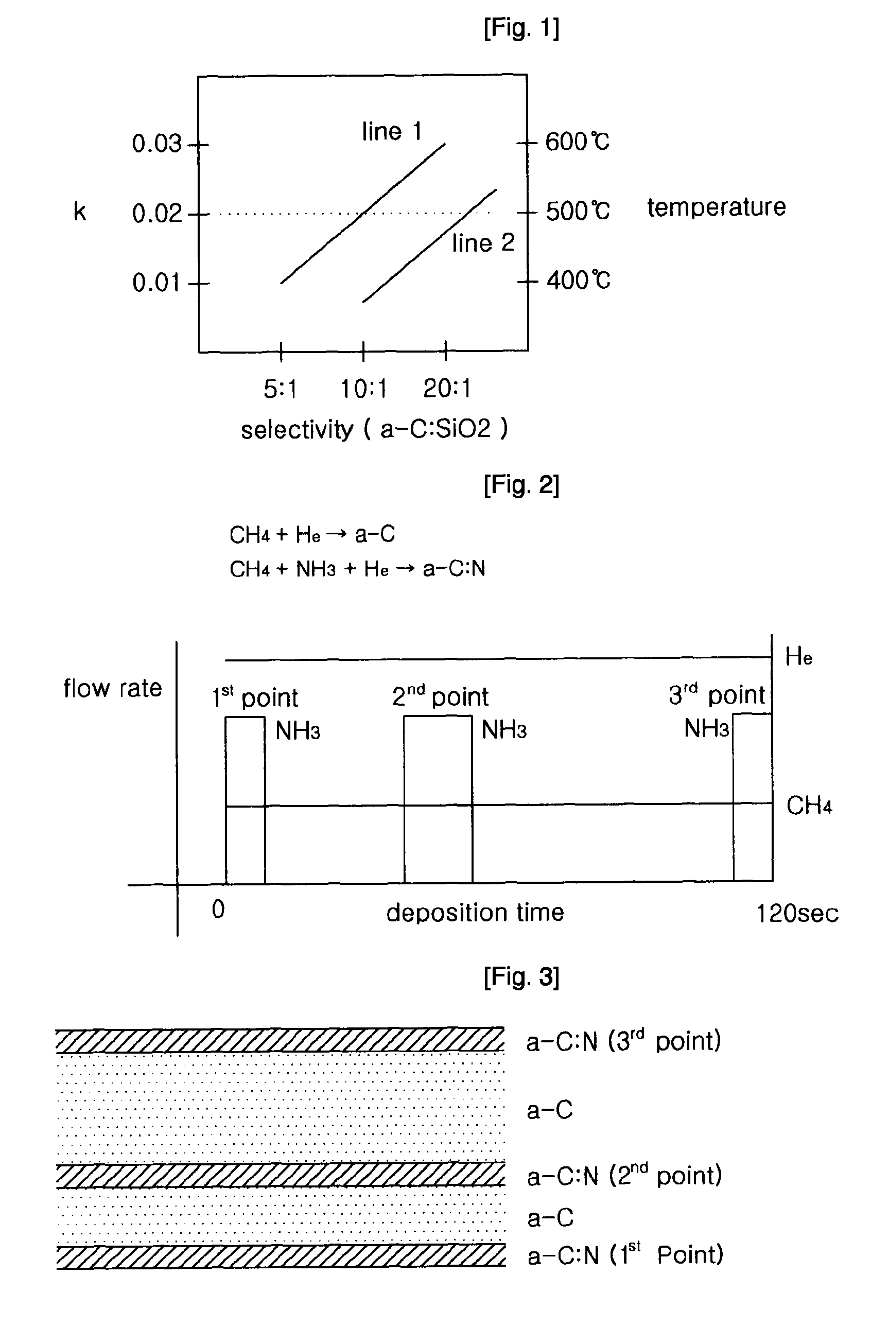
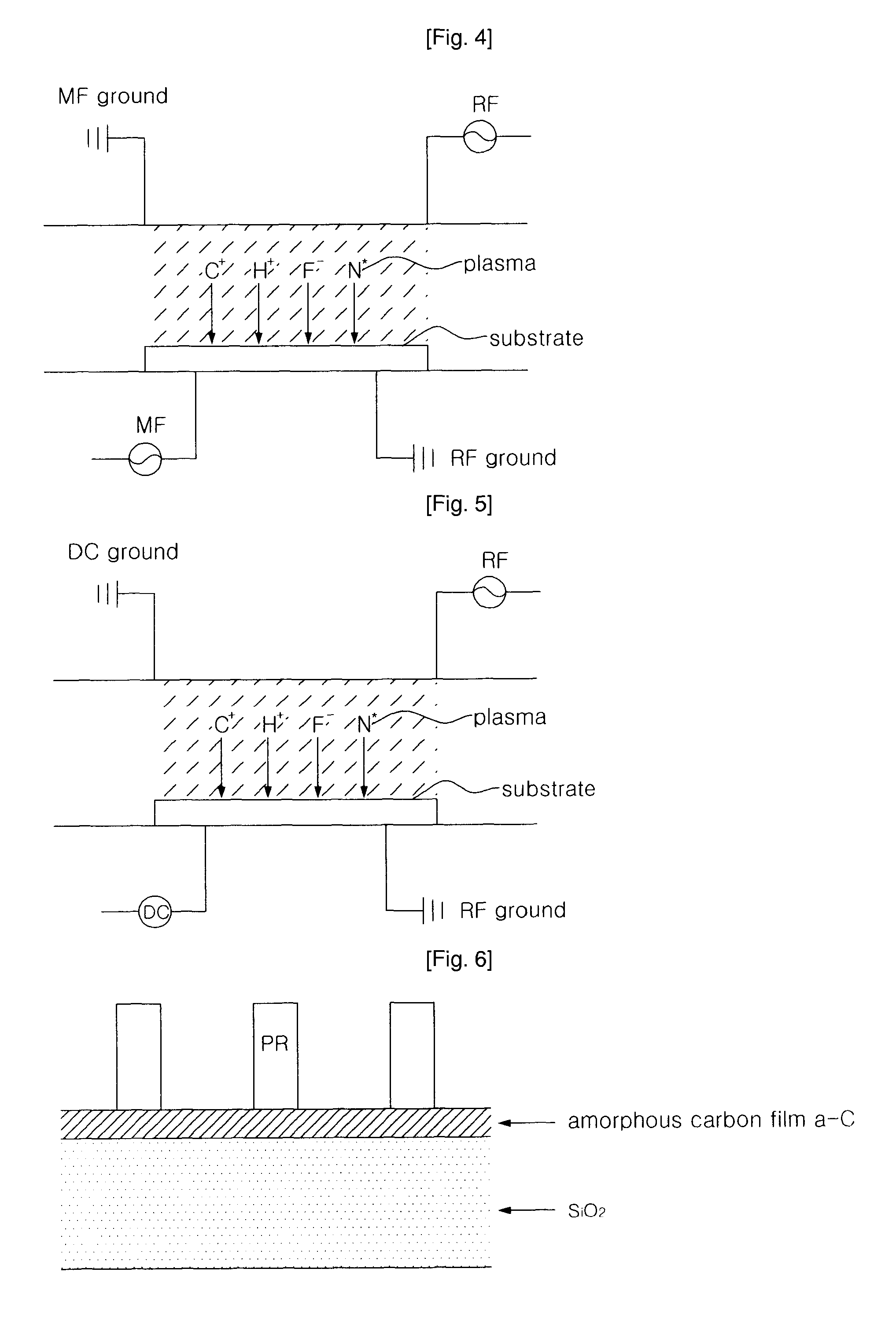
[0022]In general, an organic carbon film using plasma is formed in a manner such that a gas mixture comprising an organic gas, such as CH4, C2H6, C2H4, C2H2, C3H8, etc., and an inert gas, such as He, Ar, Ne, etc., is deposited through the application of plasma. In the common case of using a Deep UV light source of 248 nm, a thickness of about 1,500 Å is required. The optical properties of the organic carbon film depend on the total thickness of the carbon film and the bandgap of the constituent atoms thereof.

[0023]Further, the etching properties of the organic carbon film vary with the chemical reactivity of an etching gas, such as CF4 or CHF3, on the film, and the surface hardness, corresponding to resistance to ion impact.

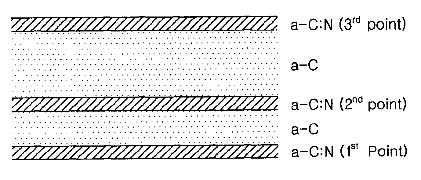
[0024]Thus, if a film of a-C:N or a-C:F may be uniformly deposited to a thickness from ones of to tens of nm on or in the organic carbon film...


PUM

PropertyMeasurementUnit
thicknessesaaaaaaaaaa
thicknessaaaaaaaaaa
thicknessaaaaaaaaaa

Abstract

Disclosed herein are a method of depositing a thin film and a method of manufacturing a semiconductor using the same, having high selectivity by increasing etching resistance while an extinction coefficient associated with anti-reflectivity is maintained low. The method of depositing a thin film according to the invention includes (a) depositing an carbon anti-reflective film on the bottom film of a substrate; and (b) adding a compound containing nitrogen (N), fluorine (F) or silicon (Si) to the surface or the inner portion of the carbon anti-reflective film, to deposit a thin film of a-C:N, a-C:F or a-C:Si, having high selectivity, to a thickness from 1 to 100 nm using an atomic layer deposition process. Therefore, an ultrathin film having etching resistance is formed on or in the carbon anti-reflective film and the density and compressive stress of the carbon anti-reflective film are increased, thus increasing etching selectivity.

Description

TECHNICAL FIELD[0001]The present invention relates generally to a method of manufacturing a semiconductor device, and, more particularly, to a method of manufacturing a semiconductor device using an amorphous carbon anti-reflective film.BACKGROUND ART[0002]Since the degree of integration of almost all highly integrated semiconductor devices having high capacities, such as DRAMs or FRAMs, is doubled every year, the degree of difficulty encountered in semiconductor manufacturing processes is further increasing.[0003]In particular, since a design rule required for a pattern formation process for use in the formation of fine pattern becomes small, it is important to suppress variations in notching or critical dimensions generated during the pattern formation process.[0004]To this end, an anti-reflective film having a low refractive index should be deposited on a bottom film which is to be patterned, to minimize the irregular reflection or diffraction of radiated light of 365 nm or 248 n...

Claims


Application Information

Patent Timeline
Patent Type & Authority Patents(United States)
IPC IPC(8): H01L21/4763H01L21/02
CPCG03F7/091H01L21/0276H01L21/3146Y10S438/952H01L21/02321H01L21/0228H01L21/02205H01L21/02274H01L21/02115H01L21/022H01L21/31H01L21/205
Inventor LEE, KI HOONPARK, YOUNG HOONLEE, SAHNG KYOOSEO, TAE WOOKCHANG, HO SEUNG
Owner WONIK IPS CO LTD
Why Eureka
Try Eureka