Low noise amplifier

a low-noise amplifier and amplifier technology, applied in the direction of low-noise amplifiers, high-frequency amplifiers, rf amplifiers, etc., can solve the problems of easy oscillation, increase in the number of parts, increase in the area of printed circuit boards, etc., to improve the input impedance matching of an lna, high dynamic range, and high gain of the feedback loop

Inactive Publication Date: 2010-11-30
ICOM INC
View PDF9 Cites 11 Cited by
  • Summary
  • Abstract
  • Description
  • Claims
  • Application Information

AI Technical Summary

Benefits of technology

[0031]Accordingly, it is an object of the present invention to provide an LNA which can keep its noise figure lower than conventional LNAs, while maintaining its feedback loop gain high, across a wide frequency band. Further, it is another object of the present invention to show a method to improve the input impedance matching of an LNA having a high dynamic range, in a high frequency band.

Problems solved by technology

However, the trade-off between providing a high feedback loop gain and increasing the cut-off frequency of the feedback loop gain raises a problem such that if a high feedback loop gain is held up to a high frequency band, applying the conventional compensation approach to the LNA cannot provide sufficient phase compensation, resulting in easy oscillation, so that the LNA does not serve as an amplifier.
From the viewpoint of the cost restriction, it is not possible to form a capacitor with such a large capacitance on an integrated network.
This requires that the capacitor 11 should be an external part, which disadvantageously leads to an increase in the number of parts and an increase in the printed circuit board area.
This is one drawback of the dominant-pole compensation method.
The band where a high feedback loop gain can be maintained is limited to a frequency significantly lower than the upper limit of the transformer passband, so that the LNA, if used for high frequency applications, cannot demonstrate a substantial performance.
This is another drawback of the dominant-pole compensation method.
In the LNA using the dominant-pole compensation method, as mentioned above, it is difficult to keep a high feedback loop gain at a high frequency band.
Therefore, the LNA in FIG. 20 is not suitable for use as a high-frequency LNA, which demands a wide dynamic range.
In case of carrying out phase compensation by making the capacitance of the phase compensation capacitor larger to reduce the cut-off frequency of the feedback loop gain, the zero of the feedback loop transfer function shifts to the low frequency side at the same time, so that the cross-over frequency falls insufficiently, thus disabling the stabilization of the LNA.
The above situations make it difficult to achieve phase compensation of the LNA having a high dynamic range.

Method used


Image

  • Low noise amplifier
  • Low noise amplifier
  • Low noise amplifier

Examples


first embodiment

[0074]Referring to the accompanying drawings, a first embodiment of the present invention is described below in detail.

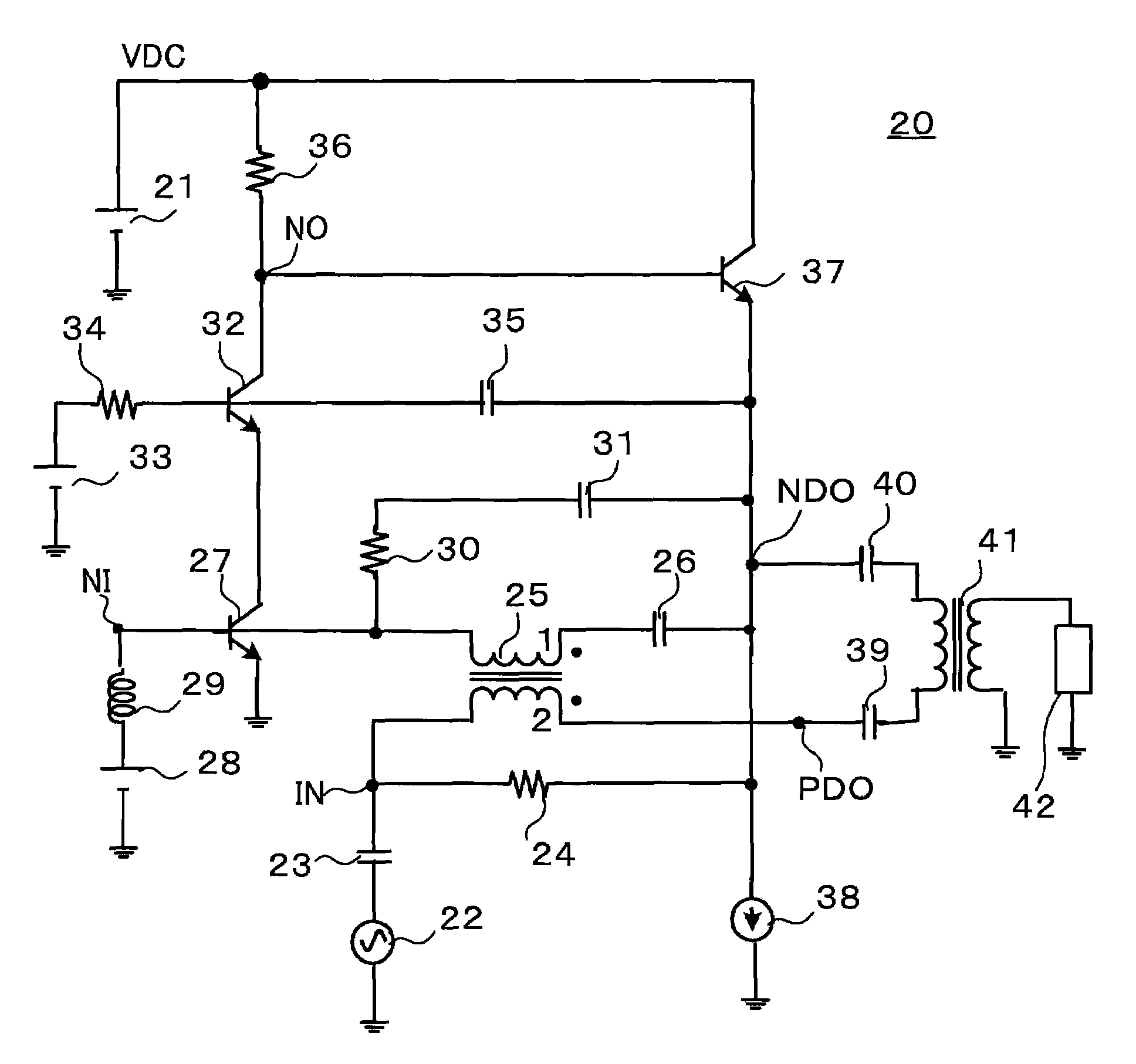
[0075]As shown in FIG. 1, an LNA 20 according to the first embodiment of the invention is a cascode type amplifier, which has a double negative feedback circuit including a transformer and a resistor. The LNA 20 is configured by using transistors with a gain bandwidth fT of 8 GHz, and operates on a DC supply voltage VDC of 10 V supplied from the DC voltage source 21.

[0076]The design specifications of the LNA 20 include a voltage gain of about 2 dB, a maximum feedback loop gain of 40 dB or higher, a phase margin of 30 degrees or greater, and are intended to be suitable for use in a case where an intense interfering signal input is present and a low gain, low distortion and a low noise figure are simultaneously demanded.

[0077]In the LNA 20, a signal source 22 with an output impedance of 50Ω is connected via a capacitor 23 to an input terminal IN to which one end of a ...

second embodiment

[0120]While the foregoing description of the first embodiment has been given of the LNA 20, which hardly has a voltage gain (2 dB or lower), the embodiment cannot be adapted to a case where a meaningful amount of voltage gain is needed. The following description of a second embodiment is given of an LNA 20A, which has a higher voltage gain.

[0121]As shown in FIG. 6, like the LNA 20 in FIG. 1, the LNA 20A according to the second embodiment of the invention operates on the DC supply voltage VDC of 10 V supplied from the DC voltage source DCS, and is configured by using transistors with a gain bandwidth fT of 8 GHz. The design specifications include a voltage gain of about 8 dB, a maximum feedback loop gain of 40 dB or higher, and a phase margin of 30 degrees or greater.

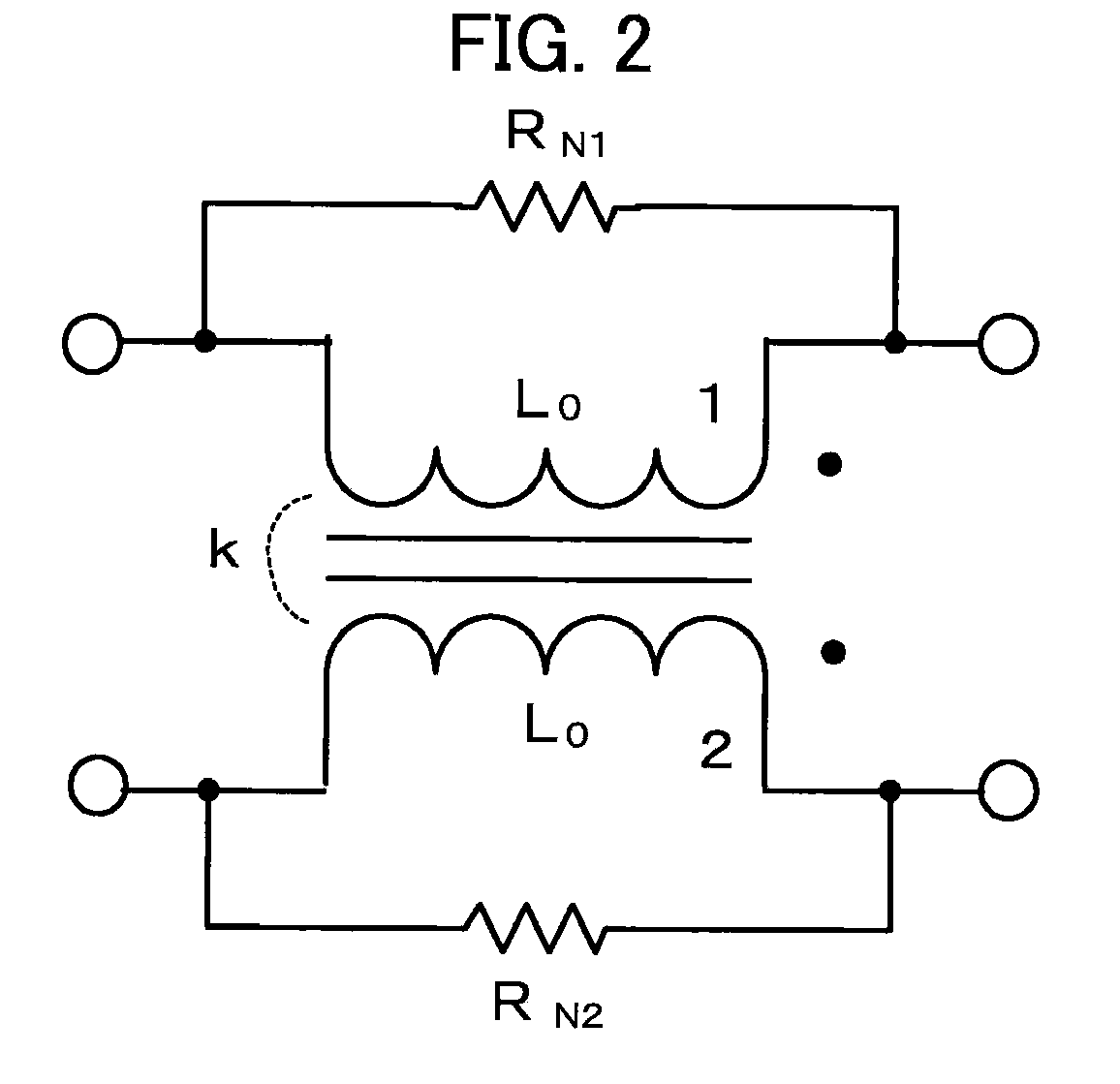
[0122]The LNA 20A uses a transformer 25X configured to have a combination of two transformers 25a and 25b in place of the transformer 25 in the LNA 20 in FIG. 1. The transformers 25a and 25b each have a turn ratio of 1:1...

third embodiment

[0139]As shown in FIG. 11, an LNA 20B according to a third embodiment of the invention is a modification to the LNA 20A in FIG. 6 to which an output buffer is added to lower the output impedance of the positive differential output terminal PDO of the LNA 20A. That is, the hot side of the secondary winding of the transformer 25b is connected via a coupling the capacitor 43 to the base of a transistor 44. The transistor 44 has a collector supplied with the DC supply voltage VDC from the DC voltage source 21, and an emitter connected to a constant current source 45.

[0140]A biasing DC voltage source 47 is connected to the base of the transistor 44 via a choke coil 46. The transistor 44 and the constant current source 45 constitute an emitter follower, which operates as an output buffer circuit. This makes it possible to reduce the value of the output impedance of the positive differential output terminal PDO which corresponds to the emitter of the transistor 44 and reduce the value of t...


PUM


Abstract

A low noise amplifier having a wide operating frequency band and a high dynamic range is provided. A transformer having a secondary winding connected between an input terminal to which an input signal is applied and a positive differential output terminal, and a primary winding connected between a negative differential output terminal and an input node is provided as a feedback circuit between a cascode amplifier circuit, which includes transistors and a resistor, and an output circuit, which includes a transistor and a constant current source. Selective use of a transformer whose leakage inductance has an adequate value as the feedback transformer can realize a low noise amplifier which has a wide operating frequency band and a high dynamic range.

Description

CROSS REFERENCE TO RELATED APPLICATIONS[0001]This application claims priority to the Japanese Patent Application No. 2008-219441, filed on Aug. 28, 2008, in the Japanese Patent Office, and is incorporated by reference in its entirety as if set forth in full.BACKGROUND[0002]1. Field of the Invention[0003]The present invention relates to a low noise amplifier, and, particularly, to a low noise amplifier with a wide dynamic range, which is used as a high-frequency amplifier for a radio communication device, an input amplifier for an A / D converter, or the like.[0004]2. Description of the Related Art[0005]As a conventional low noise amplifier, there is a cascode-connected amplifier disclosed in Unexamined Japanese Patent Application KOKAI Publication No. 2003-289226. The cascode-connected amplifier is known as a preferable circuit for adaptation to a wide-band amplifier, which is hardly affected by the parasitic capacitor of an input transistor.[0006]“HF Low Noise Amplifiers with Integra...

Claims


Application Information

Patent Timeline
Patent Type & Authority Patents(United States)
IPC IPC(8): H03F3/04
CPCH03F1/22H03F1/26H03F1/347H03F1/565H03F3/19H03F3/4508H03F3/50H03F2200/06H03F2200/09H03F2200/117H03F2200/153H03F2200/294H03F2200/36H03F2200/372H03F2200/451H03F2200/534H03F2200/537H03F2200/541H03F2203/5009
Inventor YAMAGUCHI, KOUICHIRO
Owner ICOM INC
Why Eureka
Try Eureka