Method for extending equipment uptime in ion implantation

a technology of ion implantation and equipment uptime, which is applied in the field of semiconductor manufacturing, can solve the problems of reducing the productivity (wafer throughput) reducing the efficiency of the implant tool, and reducing the performance of the nmos transistor. the effect of service life and performan

Inactive Publication Date: 2011-01-25
SEMEQUIP
View PDF187 Cites 3 Cited by
  • Summary
  • Abstract
  • Description
  • Claims
  • Application Information

AI Technical Summary

Benefits of technology

[0020]The invention features in-situ cleaning process for an ion source and associated extraction electrodes and similar components of the ion-beam producing system, which chemically removes carbon deposits, increasing service lifetime and performance, without the need to disassemble the system.
[0021]The invention features the increased reactivity of molecular implant residue with reactive gases. In particular, an aspect of the invention is directed to an activating, catalytic, or reaction promoting species added to the reactive species to effectively convert the non-volatile molecular residue into a volatile species which can be removed by conventional means.
[0022]An aspect of the invention is directed to increased rates of reaction to shorten cycle times.

Problems solved by technology

The inclusion of Ge atoms only works for PMOS transistors because compressive strain is detrimental to the electron mobility and degrades the performance of an NMOS transistor.
As device technology continues to scale in all dimensions, it becomes increasingly difficult to form the p-type Ultra Shallow Junctions, or USJ, necessary for the proper formation of the PMOS transistor.
The most challenging feature of the PMOS transistor is the Source / Drain Extension, or SDE, which must be the shallowest junction in the transistor to be effective.
The implant energy has also been reduced to make the initial dopant placement shallower, i.e., closer to the silicon surface, but since implanter beam currents are reduced at lower beam energy, and substantially so at the sub-keV boron energies required for boron implantation for sub-90 nm feature sizes, this significantly reduces the productivity (wafer throughput) of the implant tool, and so is not an attractive means to reduce junction depth.
This boron movement challenges the formation of very shallow junctions.
Both of these technologies are still immature and face significant challenges in providing production worthy solutions.
Also, as thermal budgets are reduced to very small values by these ultra-fast annealing approaches, the activation process itself is affected.
However, since the F is introduced in the same implantation process as the boron, i.e., as part of the molecular species BF3, the as-implanted F depth profile that results from BF2+ implant is not optimized for the reduction of B diffusion; this makes BF2+ implantation less attractive as junction depths are reduced further.
The use of CO2 or CO gas degrades the service lifetime of conventional plasma sources due to oxidation effects and also carbon tracking of insulators found in the sources.
The issue with the conventional technology is that the implantation by single atoms becomes very inefficient when the energy of the ions must be low (e.g., 1 or 2 keV) in order to provide for shallow implant.
Conventional systems cannot produce high currents at low extraction energy and so the implantation process has very low productivity.
However, the utilization of large molecular species, such as carbon, has introduced new challenges in removing residual matter from within the implantation device.
As such, previous cleaning methodologies have proven to be unsatisfactory in removing residual materials to acceptable levels.
Deposits of these larger “cluster” molecules do not react at sufficient rates under the previous conditions.

Method used


Image

  • Method for extending equipment uptime in ion implantation
  • Method for extending equipment uptime in ion implantation

Examples


Embodiment Construction

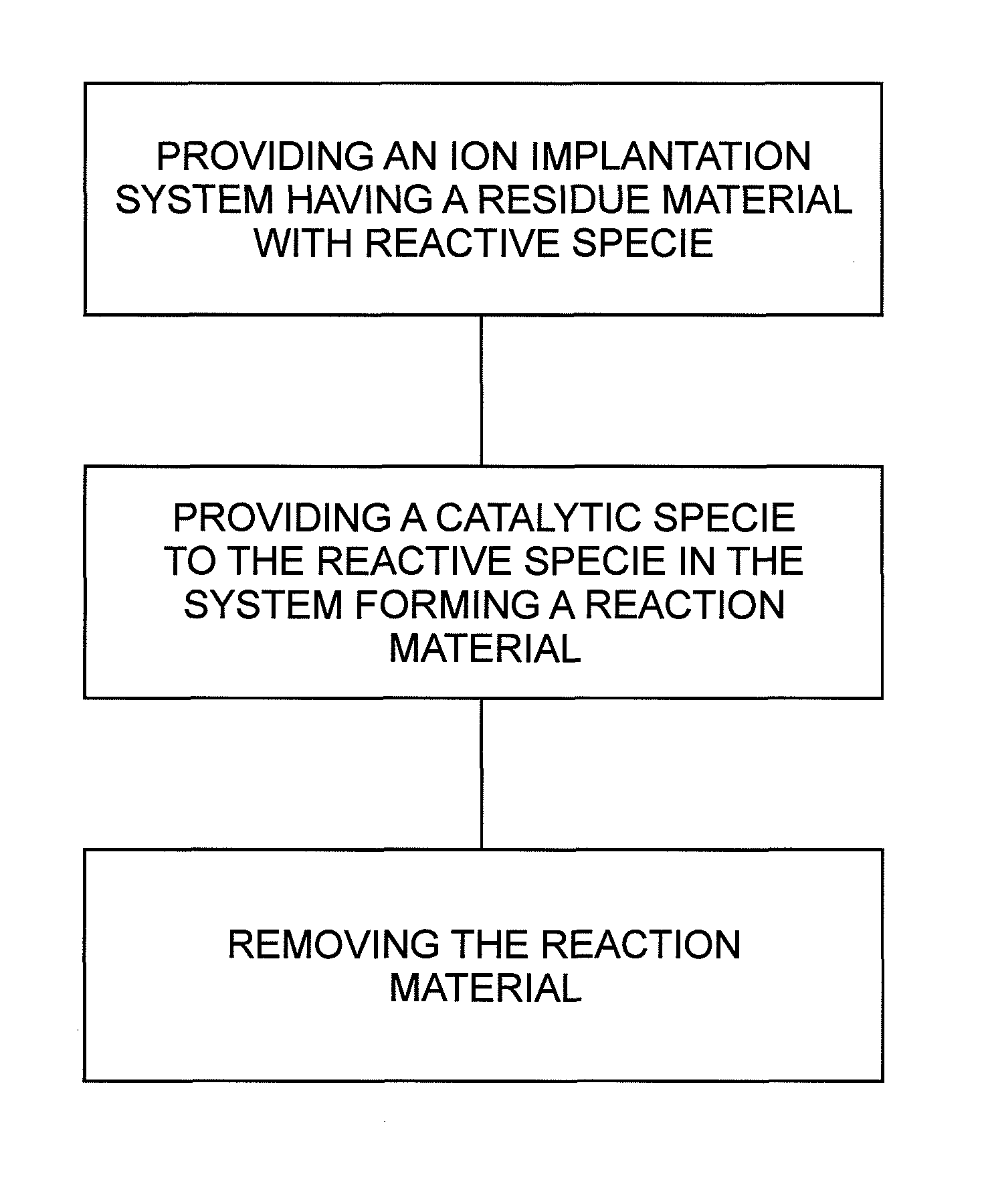
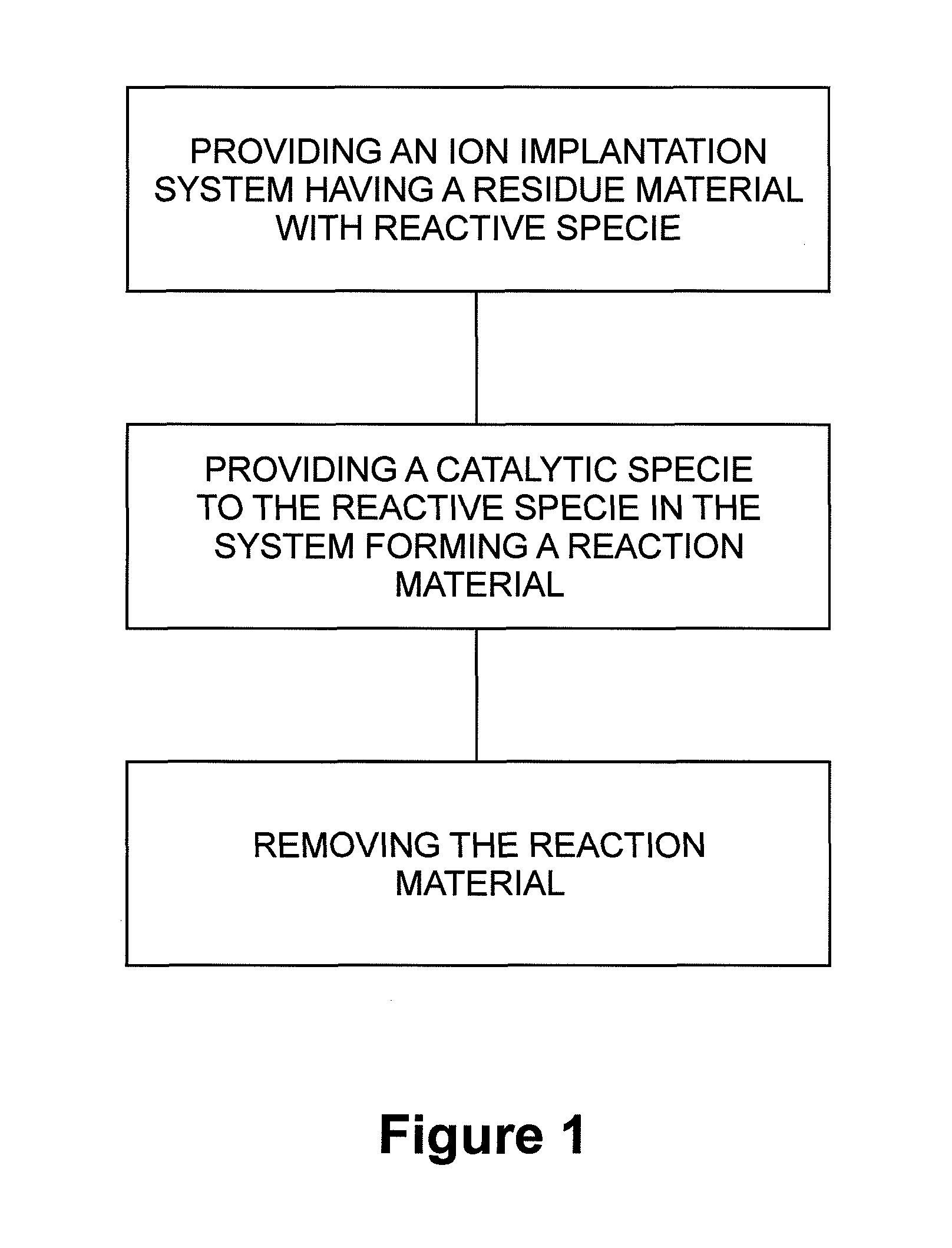
[0026]The invention comprises an improvement in cleaning of carbon residues from semiconductor wafer processing equipment, such as, an ion implantation system, wherein the carbon residue is contacted with one or more reaction species in the presence of a reaction promoting or catalytic species. The standard method used for B18 cleaning is has essentially no affect on carbon cluster residues. That is flourine F* components generated in the plasma from NF3 is not known to remove the residue build up. When B18 residue is deposited on top of or underneath carbon cluster residues and a standard cleaning recipe run, a reasonable clean was achieved. The only difference being the addition of boron hydride to the system. From an RGA analysis of the B18 clean, the boron residues are removed from the system as BF3. This byproduct of the boron clean is a so called “Lewis acid” (electron density acceptor) that is known to catalytically activate aromatic pi electron system, such as those found in...


PUM

PropertyMeasurementUnit
depthsaaaaaaaaaa
depthsaaaaaaaaaa
depthsaaaaaaaaaa

Abstract

The invention features in-situ cleaning process for an ion source and associated extraction electrodes and similar components of the ion-beam producing system, which chemically removes carbon deposits, increasing service lifetime and performance, without the need to disassemble the system. In particular, an aspect of the invention is directed to an activating, catalytic, or reaction promoting species added to the reactive species to effectively convert the non-volatile molecular residue into a volatile species which can be removed by conventional means.

Description

CROSS REFERENCE TO RELATED APPLICATIONS[0001]This application claims priority to and the benefit of U.S. Provisional Patent Application No. 60 / 974,176, filed on Sep. 21, 2007.BACKGROUND OF THE INVENTION[0002]1. Field of the Invention[0003]The present invention relates to a method of semiconductor manufacturing and more particularly to a process for removing residual, non-volatile implant material from the internal surfaces of an ion implanter system.[0004]2. Description of the Prior ArtThe Ion Implantation Process[0005]The fabrication of semiconductor devices involves, in part, the formation of transistor structures within a silicon substrate by ion implantation. As disclosed by Sferlazzo et. al. in U.S. Pat. No. 5,497,006, ion implantation equipment includes an ion source which creates a stream of ions containing a desired dopant species, a beam line which extracts and accelerates the ions from the ion source by means of an extraction electrode, and forms and focuses the ion stream...

Claims


Application Information

Patent Timeline
Patent Type & Authority Patents(United States)
IPC IPC(8): B08B5/00
CPCB08B7/0035C23C14/48C23C14/564
Inventor COOK, KEVIN S.MANNING, DENNISMCINTYRE, EDWARD K.GOLDBERG, RICHARD
Owner SEMEQUIP
Why Eureka
Try Eureka