Display device

a display device and liquid crystal technology, applied in optics, instruments, transistors, etc., can solve the problems of low current drive capability, inability to reduce frame size, and inability to electrically connect the electric capacitance between scan lines, etc., to achieve excellent electric characteristics, high yield, and high reliability

Inactive Publication Date: 2011-03-01
SEMICON ENERGY LAB CO LTD
View PDF25 Cites 19 Cited by
  • Summary
  • Abstract
  • Description
  • Claims
  • Application Information

AI Technical Summary

Benefits of technology

[0012]A thin film transistor using an amorphous semiconductor film has low carrier mobility. That is, current drive capability is low. Therefore, when a protection circuit is formed by using a thin film transistor using an amorphous semiconductor film, there is a problem in that a transistor having large size should be formed in order to sufficiently take a countermeasure against electrostatic discharge, and reduction in frame size is inhibited. Further, when a transistor having large size is formed, there is a problem in that electric capacitance between a scan line electrically connected to a gate electrode and a signal line electrically connected to a source electrode or a drain electrode is increased, whereby power consumption is increased.
[0013]A thin film transistor using a polycrystalline semiconductor film has higher mobility than a thin film transistor using an amorphous semiconductor film by two or more digits, and a pixel portion of a liquid crystal display device and a peripheral driver circuit thereof can be formed over the same substrate. However, because of crystallization of a semiconductor film, manufacturing steps of a thin film transistor using a polycrystalline semiconductor become more complicated than manufacturing steps of a thin film transistor using an amorphous semiconductor film. Therefore, there is a problem in that yield is low and cost is high.
[0014]Meanwhile, there is a problem in that the surface of a crystal grain of a microcrystalline semiconductor film is easily oxidized. Therefore, a crystal grain of a channel formation region is easily oxidized in manufacturing steps of a thin film transistor, and an oxide film is formed on the surface of the crystal grain. There is a problem in that the oxide film inhibits movement of carries and electric characteristics of the thin film transistor are decreased (for example, mobility is decreased).

Problems solved by technology

That is, current drive capability is low.
Therefore, when a protection circuit is formed by using a thin film transistor using an amorphous semiconductor film, there is a problem in that a transistor having large size should be formed in order to sufficiently take a countermeasure against electrostatic discharge, and reduction in frame size is inhibited.
Further, when a transistor having large size is formed, there is a problem in that electric capacitance between a scan line electrically connected to a gate electrode and a signal line electrically connected to a source electrode or a drain electrode is increased, whereby power consumption is increased.
However, because of crystallization of a semiconductor film, manufacturing steps of a thin film transistor using a polycrystalline semiconductor become more complicated than manufacturing steps of a thin film transistor using an amorphous semiconductor film.
Therefore, there is a problem in that yield is low and cost is high.
Meanwhile, there is a problem in that the surface of a crystal grain of a microcrystalline semiconductor film is easily oxidized.
There is a problem in that the oxide film inhibits movement of carries and electric characteristics of the thin film transistor are decreased (for example, mobility is decreased).
In addition, high voltage is often applied to a thin film transistor used for a protection circuit, and large current flows therethrough in some cases.

Method used


Image

  • Display device
  • Display device
  • Display device

Examples


embodiment mode 1

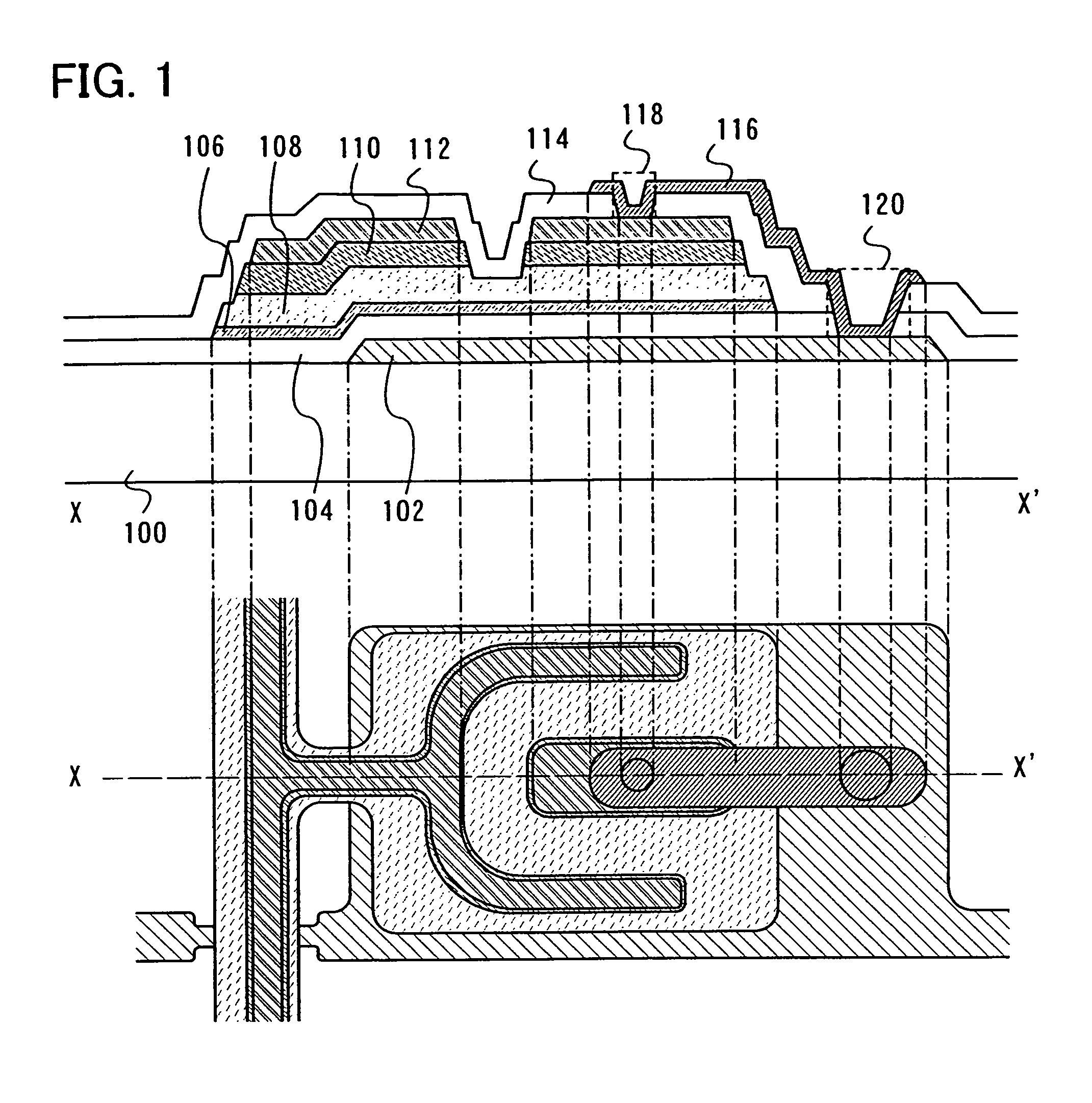
[0072]In this embodiment mode, one mode of the present invention is described with reference to the drawings.

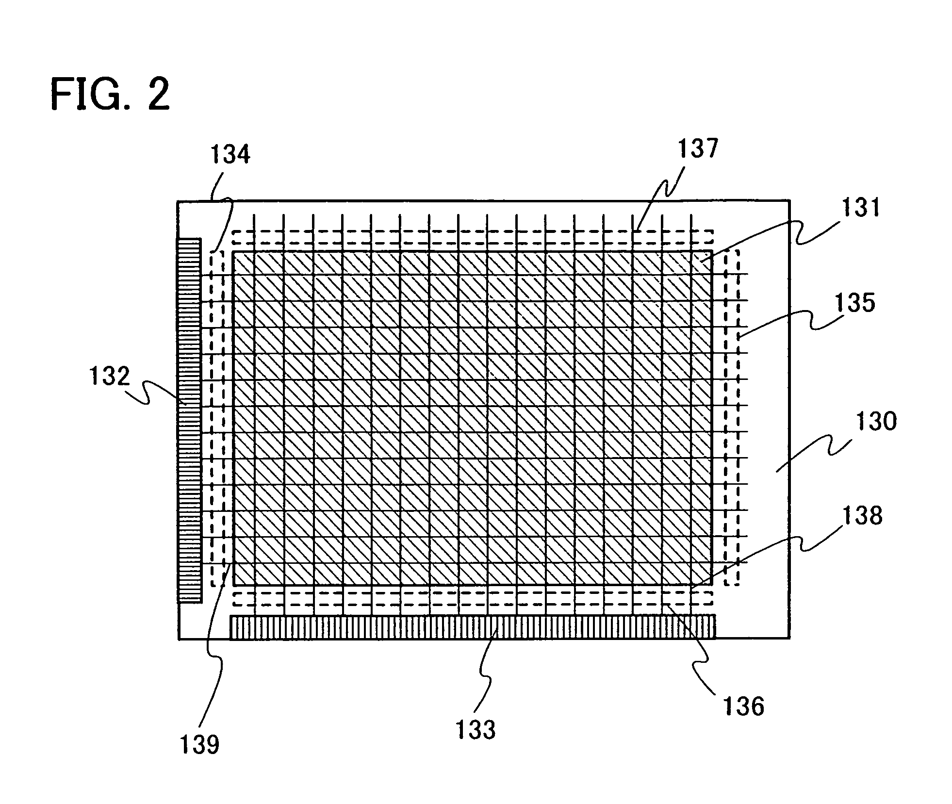
[0073]First, the structure of a semiconductor display device of the present invention is described with reference to FIG. 2. FIG. 2 is a top view of a substrate 130 over which a semiconductor display device is formed. A pixel portion 131 is formed over the substrate 130. In addition, an input terminal 132 and an input terminal 133 supply a signal and power for displaying images to a pixel circuit formed over the substrate 130.

[0074]Note that the present invention is not limited to the mode shown in FIG. 2. That is, one or both of a scan line driver circuit and a signal line driver circuit may be formed over the substrate 130.

[0075]The input terminal 132 on the scan line side and the input terminal 133 on the signal line side which are formed over the substrate 130 are connected to the pixel portion 131 by wirings extended vertically and horizontally. The wirings are connected...

embodiment mode 2

[0218]In this embodiment mode, a liquid crystal display device including a protection circuit using the thin film transistor shown in Embodiment Mode 1 is described.

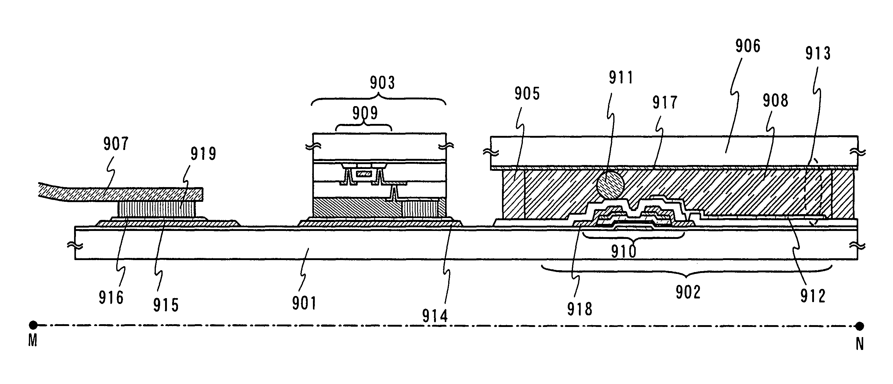
[0219]First, a VA (vertical alignment)-mode liquid crystal display device is described. A VA-mode is a mode in which liquid crystal molecules are aligned vertically to a panel surface when voltage is not applied. In particular, in this embodiment mode, it is devised that a pixel is divided into several regions (subpixels) so that molecules are aligned in different directions. This is referred to as domain multiplication or multi-domain. In the following description, a multi-domain liquid crystal display device is described.

[0220]FIG. 9 is a plan view of a side of a substrate over which a pixel electrode is formed. FIG. 8 shows a cross-sectional structure taken along the line A-B in FIG. 9. In addition, FIG. 10 is a plan view of a side of a substrate on which a counter electrode is formed. Hereinafter, description is made...

embodiment mode 3

[0264]The present invention can be applied not only to a liquid crystal display device but also a light-emitting device. In this embodiment mode, a manufacturing process and the like of light-emitting devices are described with reference to FIGS. 22A and 22B and FIGS. 23A to 23C. A light-emitting element utilizing electroluminescence is used for a light-emitting device. Light-emitting elements utilizing electroluminescence are classified according to whether a light-emitting material is an organic compound or an inorganic compound. In general, the former is referred to as organic EL elements and the latter as inorganic EL elements.

[0265]In an organic EL element, when voltage is applied to a light-emitting element, electrons and holes are injected from a pair of electrodes into a layer containing a light-emitting organic compound, and current flows. Then, recombination of these carriers (the electrons and holes) makes the light-emitting organic compound to form an excited state and t...


PUM

PropertyMeasurementUnit
diameteraaaaaaaaaa
sizesaaaaaaaaaa
sizesaaaaaaaaaa

Abstract

To provide a display device including a protection circuit having a thin film transistor which has small size and high withstand voltage. In the protection circuit of the display device, a thin film transistor is used in which an amorphous semiconductor layer, a microcrystalline semiconductor layer, a gate insulating layer which is in contact with the microcrystalline semiconductor layer, and a gate electrode layer overlap with each other. Since current drive capability of the microcrystalline semiconductor layer is high, the size of the transistor can be made small. In addition, the amorphous semiconductor layer is included, so that the withstand voltage can be improved. Here, the display device is a liquid crystal display device or a light-emitting device.

Description

BACKGROUND OF THE INVENTION[0001]1. Field of the Invention[0002]The present invention relates to a display device including a thin film transistor. In particular, the present invention relates to a liquid crystal display device or a light-emitting device.[0003]2. Description of the Related Art[0004]In recent years, a technique for forming a thin film transistor (TFT) by using a semiconductor thin film (having a thickness of approximately several to several hundreds of nanometers) formed over a substrate having an insulating surface has attracted attention. Thin film transistors have been widely applied to electronic devices such as ICs and electro-optical devices and have been rapidly developed particularly as switching elements for image display devices such as a liquid crystal display device.[0005]In a semiconductor element typified by a thin film transistor, it is one of important objects in manufacturing steps of a semiconductor device that how an electrification phenomenon (cha...

Claims


Application Information

Patent Timeline
Patent Type & Authority Patents(United States)
IPC IPC(8): H01L31/00G02F1/1368H01L21/822H01L27/04H01L29/786H01L51/50H05B33/14
CPCH01L27/0248H01L27/12H01L29/04H01L29/66765H01L29/78696H01L29/41733H01L27/1288H01L27/1248G02F1/136204H01L27/1214H01L29/458
Inventor KUROKAWA, YOSHIYUKIIKEDA, TAKAYUKI
Owner SEMICON ENERGY LAB CO LTD
Why Eureka
Try Eureka