Method for low stress flip-chip assembly of fine-pitch semiconductor devices

a technology of flip-chip interconnects and semiconductors, applied in semiconductor devices, semiconductor/solid-state device details, electrical apparatus, etc., can solve the problems of high reliability required in many applications, such as medical applications, inability to tolerate the risk of functional failure by microcracks, time-consuming fabrication flow, and incompatibility, etc., to achieve excellent electrical and thermal conductivity. the effect of high reliability

Active Publication Date: 2011-03-01
TEXAS INSTR INC
View PDF3 Cites 100 Cited by
  • Summary
  • Abstract
  • Description
  • Claims
  • Application Information

AI Technical Summary

Benefits of technology

[0010]Applicant recognized that the market trends towards higher input / output, yet thinner semiconductor devices demand the flip-assembly of ever larger chips having a pitch of the terminals, center-to-center, finer than present technology can provide. Applicant further saw that the high reliability required in many applications, such as medical applications, cannot tolerate the risk of functional failure by microcracks in the assembly connections due to thermomechanical stress. In addition, the present time-consuming fabrication flow, requiring expensive equipment for temperature and vacuum control, is incompatible with the market trend of rapidly changing customer requirements demanding short manufacturing turn-around time and low fabrication cost.
[0011]Applicant discovered that the use of high-aspect ratio connections, such as metallic columns (having for example a height of 40 μm versus a diameter of 20 μm), offers several benefits compared to the presently used low-aspect ratio connections, such as metal bumps. High-aspect ratio connections provide greater robustness for thermomechanical stress and create a wider gap between chip and substrate, thus enabling shorter process times for filling the gap with a precursor material, since the filling time is inversely proportional to the width. A wider gap further reduces the risk of incomplete filling and local voids in the underfill precursor.
[0012]In addition, high-aspect ratio connections avoid the need for various insulator (solder resist) thicknesses on the substrate surface, and for manufacturing equipment with vacuum-enhanced underfilling—advantages resulting in significant cost savings.
[0013]Applicant solved the problem of microcracks in the connections between the chips and substrate by replacing presently used low aspect-ratio connections (bumps) with high aspect-ratio connections (columns), coupled with replacing the presently used reflow solder for all-metal connections with a sinterable paste for composite connections. The paste includes copper and tin / bismuth particles, which sinter into a metallic matrix embedded in the thermoset polymeric compound; after sintering, the paste is robust and resilient against thermomechancial stress.
[0014]Selecting the paste for composite connections further replaces the present process flow of time-consuming consecutive high temperature (higher than 200° C.) cycles for the steps of reflowing the solder and curing the underfill polymer, separated by a cool-down to ambient temperature, by a process flow of a single cycle. Bonding the paste to the substrate and partially sintering the metallic matrix requires an only modestly elevated temperature (about 100° C.); at the same temperature, the step of underfillng is performed. Without cool-down, the matrix is finalized together with the curing of the underfill compound at the increased temperature of about 200° C., before the assembly is cooled to ambient temperature. The integrated manufacturing cycle minimizes thermomechanical stresses. In addition, the need for special manufacturing equipment for controlling temperature cycles is avoided.
[0016]Before polymerization and metal network formation, the sinterable paste includes a low-viscosity polymer base (such as epoxy) compound loaded with 80 to 90% metallic fillers of copper particles and alloy particles (such as bismuth and tin). The particles have a size distribution with a maximum preferably between about 3 and 10 μm. After the steps of solvent removal and of alloy sintering, the sintered paste includes a metal matrix of copper / tin intermetallics immersed in the compound. The formative steps need only 15 to 60 min. The metal matrix exhibits excellent electrical and thermal conductivities.

Problems solved by technology

Applicant further saw that the high reliability required in many applications, such as medical applications, cannot tolerate the risk of functional failure by microcracks in the assembly connections due to thermomechanical stress.
In addition, the present time-consuming fabrication flow, requiring expensive equipment for temperature and vacuum control, is incompatible with the market trend of rapidly changing customer requirements demanding short manufacturing turn-around time and low fabrication cost.

Method used


Image

  • Method for low stress flip-chip assembly of fine-pitch semiconductor devices
  • Method for low stress flip-chip assembly of fine-pitch semiconductor devices
  • Method for low stress flip-chip assembly of fine-pitch semiconductor devices

Examples


Embodiment Construction

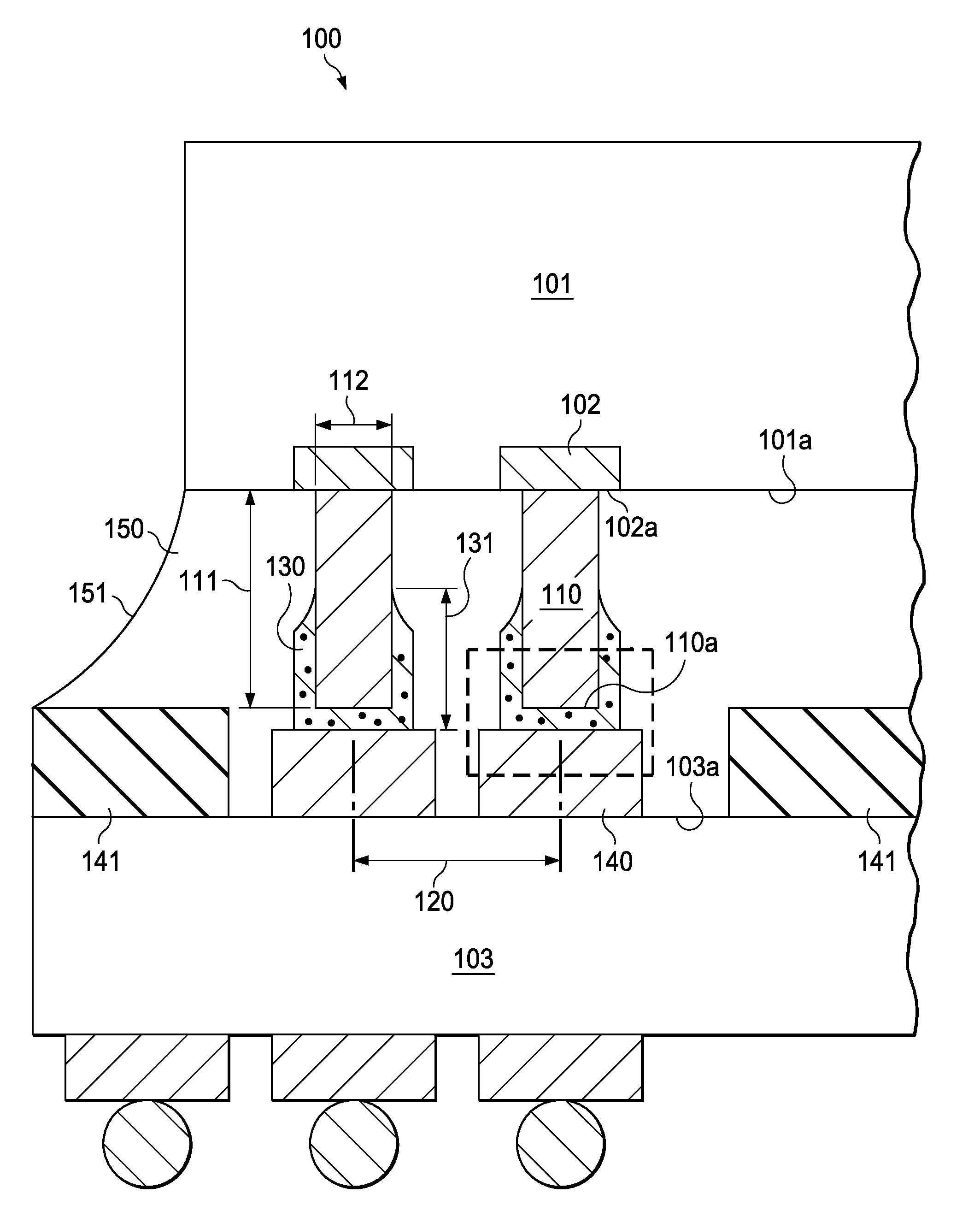
[0028]FIG. 1 illustrates an exemplary embodiment, generally designated 100, of the invention. A first body 101 with terminals 102 on the body surface 101a is assembled onto a second body 103. In a preferred embodiment of the invention, first body 101 is a semiconductor chip, terminals 102 are metal lands suitable for the attachment of connectors, which are preferably metallic, and second body 103 is an insulating substrate. As an example, terminals 102 may be lands made of copper with a metallurgical configuration of its surface 102a including a nickel layer in contact with the copper, followed by an outermost layer of gold.

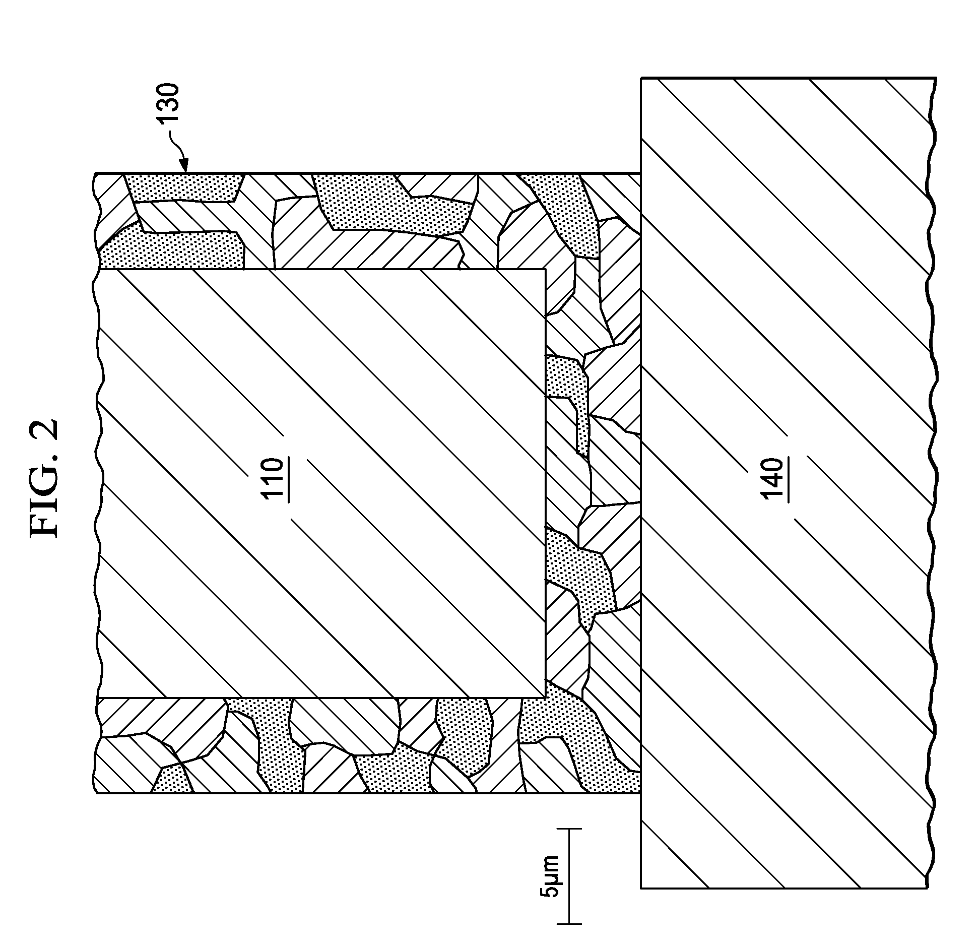
[0029]As the example of FIG. 1 shows, attached on each terminal 102 is one end of a metallic connector 110, which is shaped as a column or pillar and oriented substantially perpendicular to the surface 101a. The columnar connector 110 may have cylindrical shape or slightly conical; it has a height 111 and an average diameter 112. Preferably the aspect ratio of he...


PUM

PropertyMeasurementUnit
aspect ratioaaaaaaaaaa
temperatureaaaaaaaaaa

Abstract

A device including a first body (101) with terminals (102) on a surface (101a), each terminal having a metallic connector (110), which is shaped as a column substantially perpendicular to the surface. Preferably, the connectors have an aspect ratio of height to diameter of 2 to 1 or greater, and a fine pitch center-to-center. The connector end (110a) remote from the terminal is covered by a film (130) of a sintered paste including a metallic matrix embedded in a first polymeric compound. Further a second body (103) having metallic pads (140) facing the respective terminals (102). Each connector film (130) is in contact with the respective pad (140), whereby the first body (101) is spaced from the second body (103) with the connector columns (110) as standoff. A second polymeric compound (150) is filling the space of the standoff.

Description

FIELD OF THE INVENTION[0001]This application claims the benefit of 61 / 138,210 filed on Dec. 17, 2008.[0002]The present invention is related in general to the field of semiconductor devices and processes and more specifically to the structure and fabrication method of fine pitch flip-chip interconnects for low stress devices.DESCRIPTION OF THE RELATED ART[0003]The conventional flip-chip interconnection for attaching a semiconductor chip with a terminal pad to a substrate with a contact pad includes either a solder ball attached to the terminal pad and to the contact pad, or a gold (or copper) bump on the terminal pad connected to the solder on the contact pad, or to the gold-clad contact pad. Consequently, the sequence of terminal pad-interconnection-contact pad is an all-metal connection. The material for the chip may be silicon with a coefficient of thermal expansion (CTE) of about 2 ppm / ° C., and for the substrate a ceramic or polymer compound with a CTE of about 15 to 22 ppm / ° C....

Claims


Application Information

Patent Timeline
Patent Type & Authority Patents(United States)
IPC IPC(8): H01L23/48H01L23/52H01L29/40
CPCH01L24/11H01L2224/81191H01L2224/13099H01L2224/13147H01L2224/8184H01L2924/01029H01L2924/01032H01L2924/01047H01L2924/01061H01L2924/01078H01L2924/01079H01L2924/01082H01L2924/01322H01L2924/01327H01L2924/14H01L2924/15311H01L2224/16225H01L2224/32225H01L2224/73204H01L2924/01006H01L2924/01019H01L2924/01033H01L2924/014H01L2224/1147H01L2924/00013H01L2224/13566H01L2224/11822H01L2224/83862H01L2224/9205H01L2224/92125H01L2924/1461H01L2224/83104H01L2924/00H01L2224/29099H01L24/05H01L24/13H01L24/16H01L24/32H01L2224/0401H01L2224/0554H01L2224/05571H01L2224/05573H01L2224/056H01L2224/1379H01L2224/13811H01L2224/13847H01L2224/16238H01L2924/00014H01L2924/01083H01L2224/05599H01L2224/0555H01L2224/0556H01L2224/0557
Inventor CASTRO, ABRAM M
Owner TEXAS INSTR INC
Why Eureka
Try Eureka