Nitride semiconductor device and manufacturing method thereof

a technology of semiconductor devices and semiconductor layers, applied in semiconductor devices, semiconductor lasers, lasers, etc., can solve the problems of increased operating voltage, electron overflow, increased operating current, etc., and achieve the effect of reducing the concentration of residual hydrogen in the p-type semiconductor layer

Active Publication Date: 2011-03-29
PANASONIC CORP
View PDF9 Cites 0 Cited by
  • Summary
  • Abstract
  • Description
  • Claims
  • Application Information

AI Technical Summary

Benefits of technology

[0011]In the above conventional nitride semiconductor device, however, the p-type layer has residual hydrogen on the order of about 1017 cm−3 to about 1018 cm−3 even after the above activation process. Such residual hydrogen reduces the acceptor activation ratio and increases the resistance of the p-type layer and the contact resistance between the p-type layer and the p-side electrode, causing increase in operating voltage. In a semiconductor device having a pn junction such as a semiconductor laser device or an LED, reduction in acceptor activation ratio in a p-type layer increases electron overflow, causing increase in operating current.

Problems solved by technology

Such residual hydrogen reduces the acceptor activation ratio and increases the resistance of the p-type layer and the contact resistance between the p-type layer and the p-side electrode, causing increase in operating voltage.
In a semiconductor device having a pn junction such as a semiconductor laser device or an LED, reduction in acceptor activation ratio in a p-type layer increases electron overflow, causing increase in operating current.
Such increase in operating voltage and increase in operating current affect the efficiency and reliability of a nitride semiconductor device, and desired optical output and life cannot be obtained.
However, such a method produces defects such as nitrogen holes in the active layer or the like and thus reduces the hole concentration in the p-type layer, thereby causing increase in operating voltage and increase in operating current.
In other words, it is extremely difficult to completely remove residual hydrogen by the conventional activation processes.
In conventional nitride semiconductor devices, residual hydrogen after an activation process has a significant impact on efficiency and reliability of the semiconductor devices, hindering increase in power and life of nitride semiconductor devices.

Method used


Image

  • Nitride semiconductor device and manufacturing method thereof
  • Nitride semiconductor device and manufacturing method thereof
  • Nitride semiconductor device and manufacturing method thereof

Examples


first embodiment

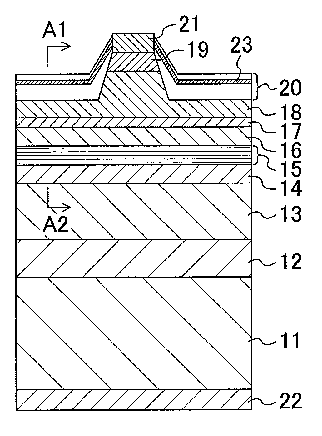
[0037]Hereinafter, a nitride semiconductor device according to a first embodiment of the present invention will be described with reference to the accompanying drawings.

[0038]FIG. 1 is a diagram showing a cross-sectional structure of a semiconductor laser device (nitride semiconductor device) according to the first embodiment of the present invention. As shown in FIG. 1, in the semiconductor laser device of the present embodiment, an n-type GaN layer 12, an n-type cladding layer 13 made of n-type AlGaN, an n-type optical guide layer 14 made of n-type GaN, a multiple quantum well active layer 15 made of InGaN, a p-type optical guide layer 16 made of p-type GaN, an electron blocking layer 17 made of p-type AlGaN, a p-type cladding layer 18, and a contact layer 19 made of p-type GaN are sequentially formed from bottom to top on a top surface of an n-type GaN substrate 11. Note that operation as a semiconductor laser device is not affected even when the p-type optical guide layer 16 and...

second embodiment

[0087]A nitride semiconductor device according to a second embodiment of the present invention will now be described with reference to the figures.

[0088]FIG. 7 shows a cross-sectional structure of the semiconductor laser device of the second embodiment. Note that FIG. 1 shows a longitudinal section vertical to the ridge waveguide (a longitudinal section vertical to the light emitting direction), while FIG. 7 shows a longitudinal section parallel to a ridge waveguide near a light emitting end on the front side of the semiconductor laser device (a longitudinal section parallel to the light emitting direction).

[0089]In the semiconductor laser device shown in FIG. 7, the structure of an n-type GaN substrate 11, an n-type GaN layer 12, an n-type cladding layer 13, an n-type optical guide layer 14, a multiple quantum well active layer 15, a p-type optical guide layer 16, an electron blocking layer 17, a p-type cladding layer 18, a contact layer 19, a p-side electrode 21, and an n-side ele...

third embodiment

[0103]A nitride semiconductor device according to a third embodiment of the present invention will now be described with reference to the figures.

[0104]FIG. 9 shows a cross-sectional structure of a semiconductor laser device according to the third embodiment. More specifically, FIG. 9 shows a longitudinal section parallel to a ridge waveguide near a light emitting end on the front side of the semiconductor laser device (a longitudinal section parallel to the light emitting direction). The semiconductor laser device of FIG. 9 has the same structure as that of the semiconductor laser device of the second embodiment shown in FIG. 7 except for a second impurity region 23b.

[0105]The semiconductor laser device of the present embodiment is characterized in that the second impurity region 23b containing fluorine is formed near the mirror face 24 that is an interface between the insulating film 30 and each nitride semiconductor layer.

[0106]In a B1-B2 section, the second impurity region 23b ...


PUM

PropertyMeasurementUnit
temperatureaaaaaaaaaa
widthaaaaaaaaaa
lengthaaaaaaaaaa

Abstract

A nitride semiconductor device includes: a semiconductor substrate; a p-type semiconductor layer formed over the semiconductor substrate, made of a nitride semiconductor, and containing first impurities; and an insulating film contacting the p-type semiconductor layer and having an impurity region containing second impurities for trapping hydrogen. Since residual hydrogen in the p-type semiconductor layer is trapped in the impurity region, the hydrogen concentration in the impurity region is higher than that in the insulating film excluding the impurity region.

Description

CROSS REFERENCE TO RELATED APPLICATION[0001]This application claims priority under 35 U.S.C. §119(a) on Japanese Patent Application No. 2007-306929 filed on Nov. 28, 2007, the entire contents of which are hereby incorporated by reference.BACKGROUND OF THE INVENTION[0002]1. Field of the Invention[0003]The present invention relates to a nitride semiconductor device such as a light emitting device like a laser diode (LD) and a light emitting diode (LED), a light receiving device like a photodiode, and an electronic device like a transistor. More particularly, the present invention relates to a nitride semiconductor device having a p-type layer.[0004]2. Related Art[0005]A nitride semiconductor has been used as a material of a light emitting device such as a laser diode and a light emitting diode.[0006]FIG. 11 is a cross-sectional view of a conventional nitride semiconductor functioning as a laser device, which is described in Japanese Laid-Open Patent Publication No. 2001-148357. As sho...

Claims


Application Information

Patent Timeline
Patent Type & Authority Patents(United States)
IPC IPC(8): H01L33/00H01S5/028H01S5/22
CPCB82Y20/00H01S5/162H01S5/22H01L33/44H01S5/028H01S5/2004H01S5/2201H01S5/2214H01S5/305H01S5/3063H01S5/3213H01S5/34333
Inventor ISHIDA, MASAHIRO
Owner PANASONIC CORP
Why Eureka
Try Eureka