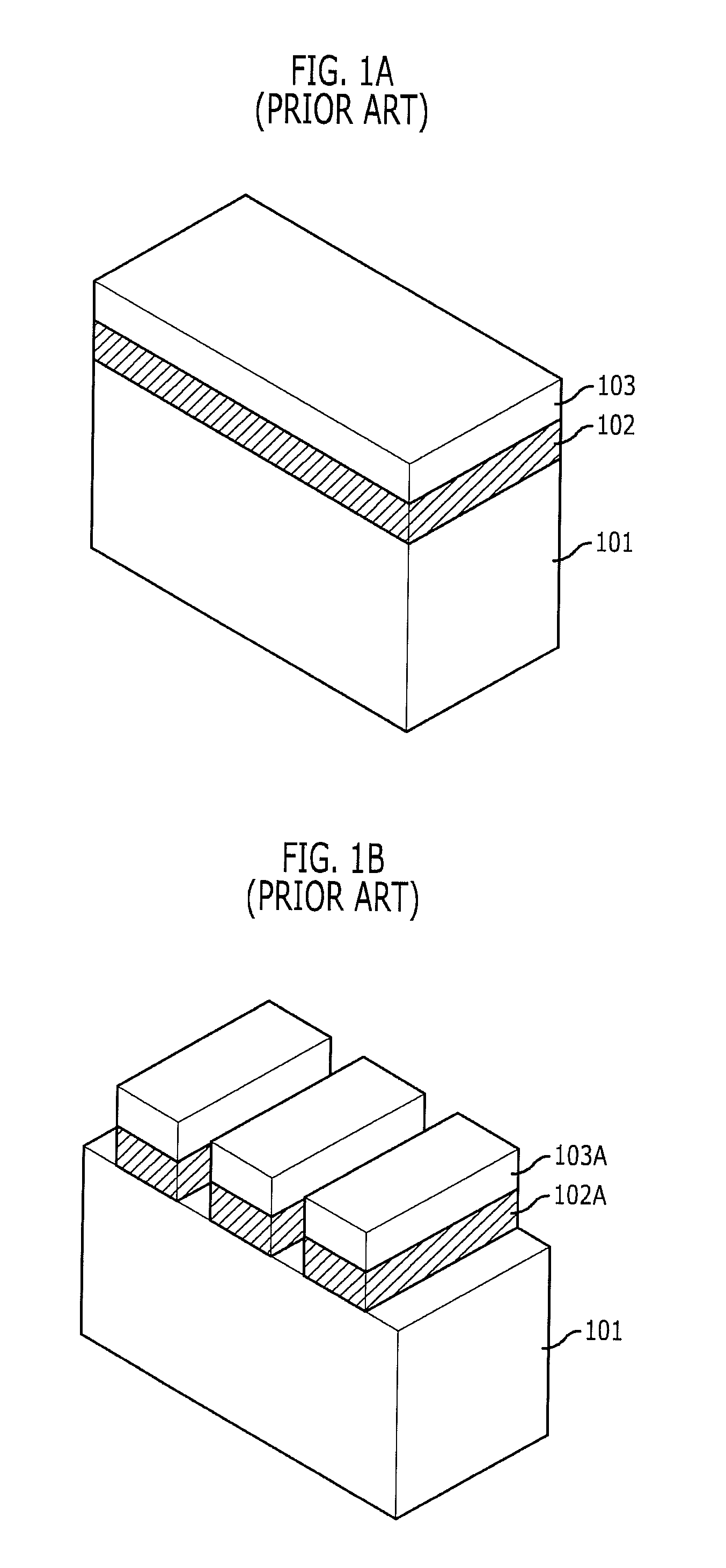
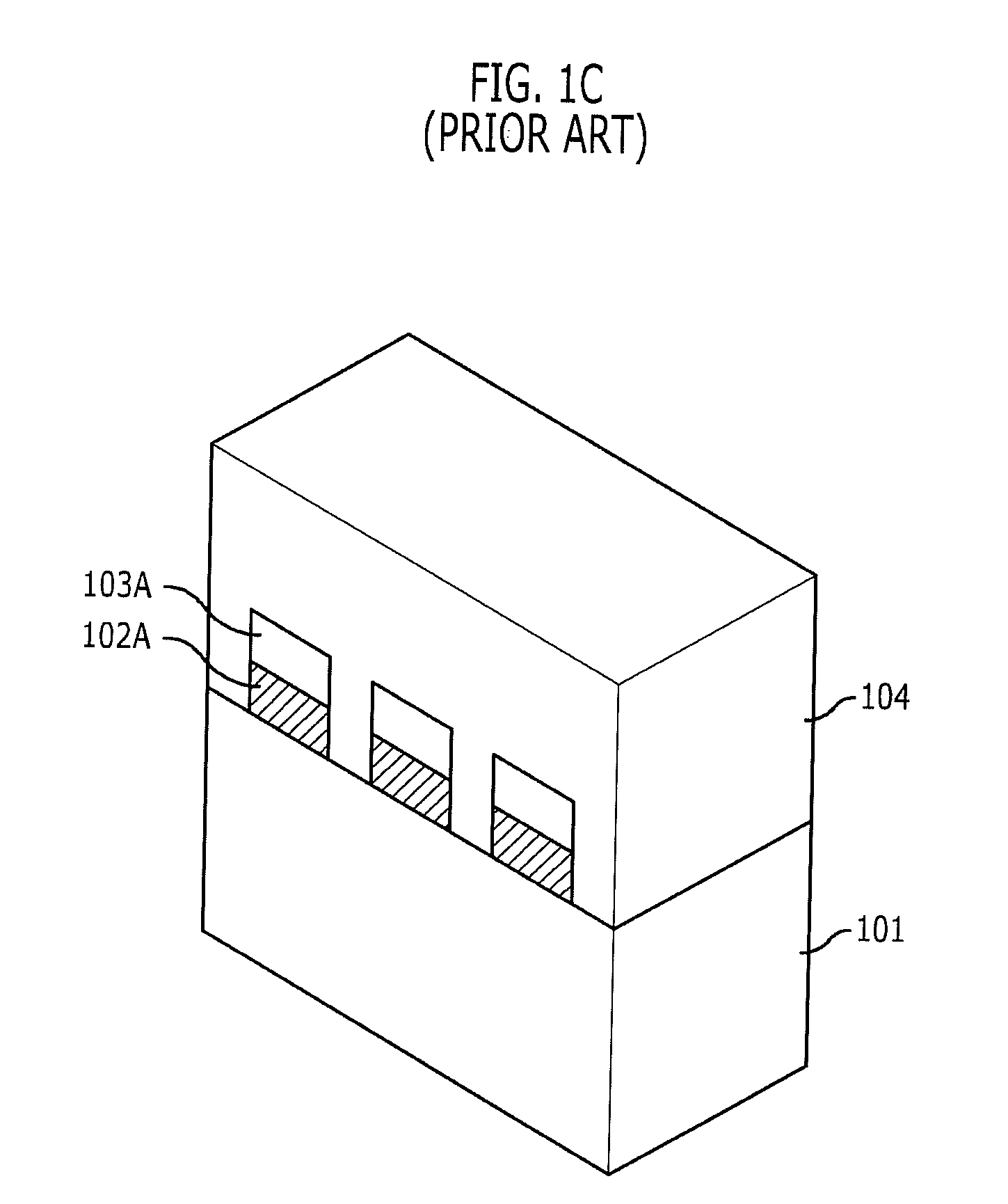
Method for fabricating partial SOI substrate
a technology of silicon germanium and substrate, which is applied in the direction of semiconductor devices, electrical equipment, basic electric elements, etc., can solve the problems of deterioration of the layer quality, high temperature may not be applied to the silicon germanium pattern, and increase the process cost, so as to reduce the diffusion
- Summary
- Abstract
- Description
- Claims
- Application Information
AI Technical Summary
Benefits of technology
Problems solved by technology
Method used
Image

Examples
first embodiment
[0044]FIGS. 2A to 2H illustrate cross-sectional views of a method for fabricating a partial SOI substrate in accordance with the present invention.
[0045]Referring to FIG. 2A, an insulation layer 202 is formed over a first silicon layer 201. The insulation layer 202 is formed to form a subsequent partial SOI. For instance, the insulation layer 202 may include a layer including a nonmetallic element. In particular, the insulation layer 202 may include an oxide-based layer. The insulation layer 202 may be formed using a method selected from a group consisting of a chemical vapor deposition (CVD) method, a physical vapor deposition (PVD) method and an atomic layer deposition (ALD) method.
[0046]An anti-reflective coating layer 203 is formed over the insulation layer 202. The anti-reflective coating layer 203 is formed to reduce reflection during a photo-exposure process when forming a first photoresist pattern 204.
[0047]A hard mask layer may be additionally formed to secure an etch margi...
second embodiment
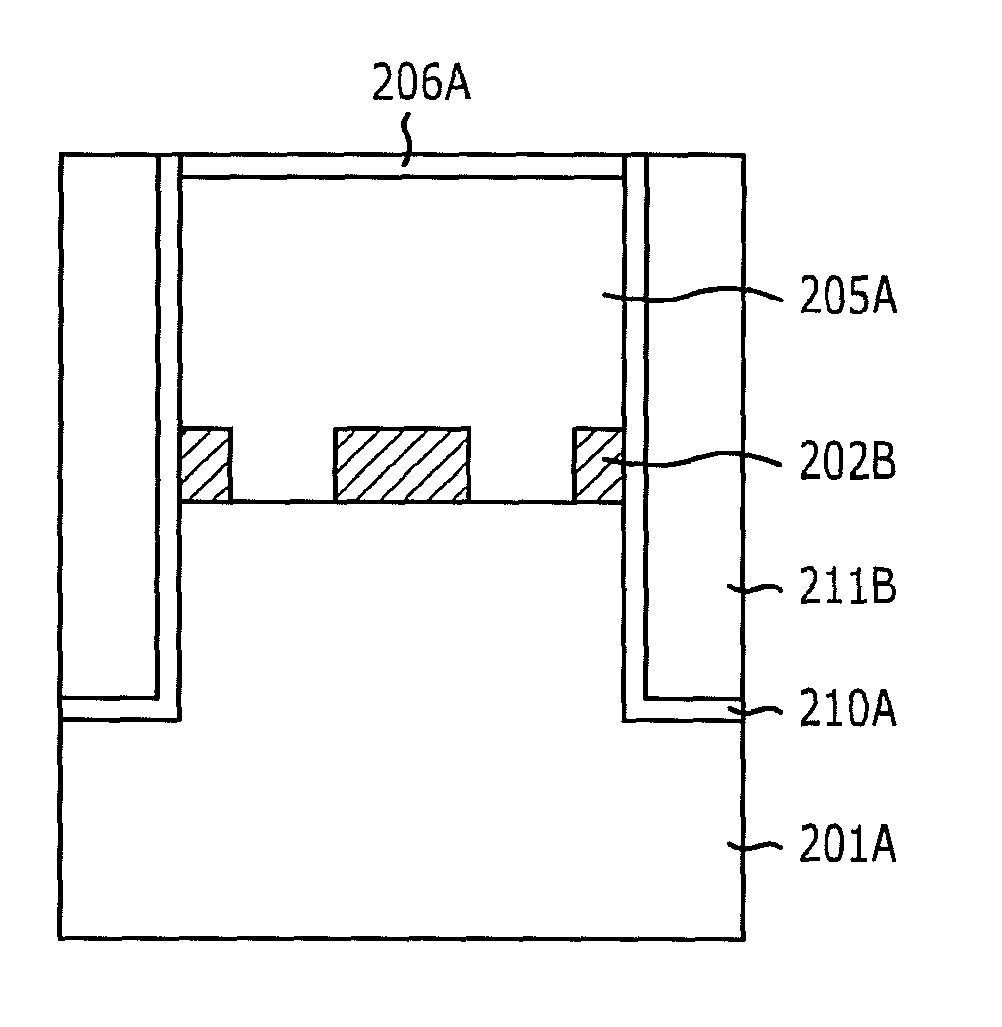
[0069]FIGS. 3A to 3I illustrate cross-sectional views of a method for fabricating a partial SOI substrate in accordance with the present invention.
[0070]Referring to FIG. 3A, a sacrificial layer 302 is formed over a first silicon layer 301. The sacrificial layer 302 is formed to form a subsequent partial SOI. For instance, the sacrificial layer 302 may include a layer including a nonmetallic element. For instance, the sacrificial layer 302 may include a material which has a high wet etch rate with respect to the first silicon layer 301 and a subsequent second silicon layer, as well as having a high wet etch rate with respect to a subsequent pad nitride layer.
[0071]The sacrificial layer 302 may be formed using a method selected from a group consisting of a chemical vapor deposition (CVD) method, a physical vapor deposition (PVD) method, and an atomic layer deposition (ALD) method.
[0072]An anti-reflective coating layer 303 is formed over the sacrificial layer 302. The anti-reflective ...
third embodiment
[0094]FIGS. 4A to 15B illustrate cross-sectional views of a method for fabricating a partial SOI substrate in accordance with the present invention. FIGS. 4A, 5A, 6A, 7A, 8A, 9A, 10A, 11A, 12A, 13A, 14A, and 15A show plan view layouts of the method for fabricating a partial SOI substrate, and FIGS. 4B, 5B, 6B, 7B, 8B, 9B, 10B, 11B, 12B, 13B, 14B, and 15B show sectional views of the method for fabricating a partial SOI substrate taken along a line I-I′. The plan view layouts and the sectional views are shown side by side for convenience of description.
[0095]Referring to FIGS. 4A and 4B, a sacrificial layer 402 is formed over a first silicon layer 401. The sacrificial layer 402 is formed to form a subsequent partial SOI. For instance, the sacrificial layer 402 may include a layer including a nonmetallic element. In particular, the sacrificial layer 402 may be formed using a material having a high wet etch rate with respect to the first silicon layer 401. For instance, the sacrificial ...
PUM
| Property | Measurement | Unit |
|---|---|---|
| temperature | aaaaa | aaaaa |
| temperature | aaaaa | aaaaa |
| shape | aaaaa | aaaaa |
Abstract
Description
Claims
Application Information