

Organic light-emitting display device
a display device and organic technology, applied in the direction of organic semiconductor devices, printing,filing appliances, etc., can solve the problems of unavoidable light emission voltage rise, oxidation of organic films, and elevated light emission voltag
- Summary
- Abstract
- Description
- Claims
- Application Information
AI Technical Summary
Benefits of technology
Problems solved by technology
Method used
Image

Examples
example 1
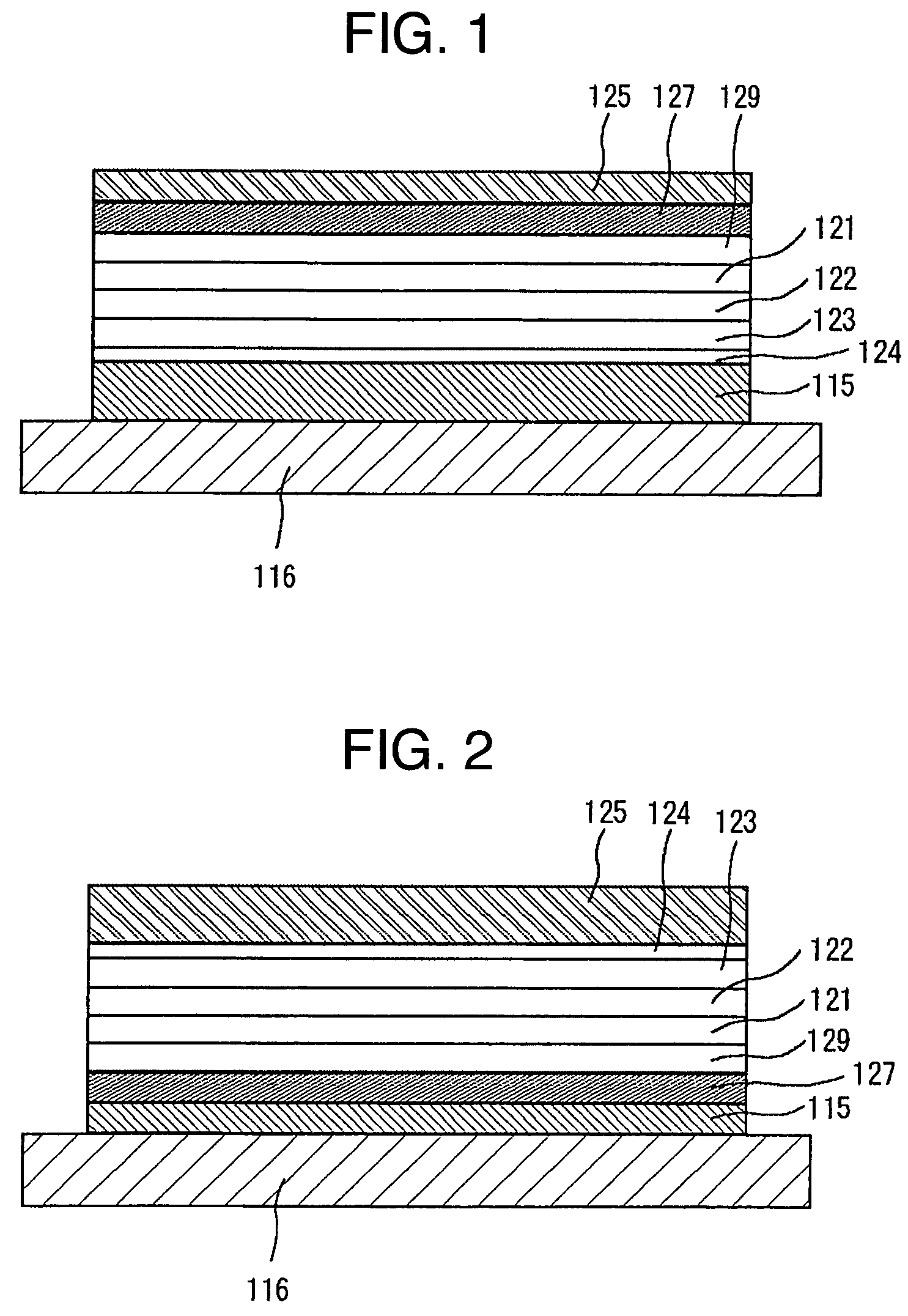
[0087]An example of organic light-emitting display device according to the present invention is explained below. FIG. 1 is a sectional view of the organic light-emitting display device according to Example 1 of the present invention. The lower electrode 115 comprises an Al film formed by EB deposition. The electrode film was patterned by using a shadow mask, and its thickness was 100 nm.
[0088]On the lower electrode 115 was formed a 0.5 nm thick LiF film as an electron injection layer 124 by vacuum deposition using a shadow mask for patterning.
[0089]On the electron injection layer 124, a film of tris(8-quinolinol) aluminum (hereinafter abbreviated as Alq), 20 nm thick, was formed by vacuum deposition. This Alq film functions as an electron transport layer 123. During the formation of the electron transport layer 123, a shadow mask was used to form its pattern. On the electron transport layer 123, a 20 nm thick co-deposition film of Alq and quinacridone (hereinafter abbreviated as Qc)...
example 2
[0096]Another example of organic light-emitting display device of the present invention is explained below. An organic light-emitting display device same as Example 1 in structure but different in thickness of the buffer layer was fabricated.
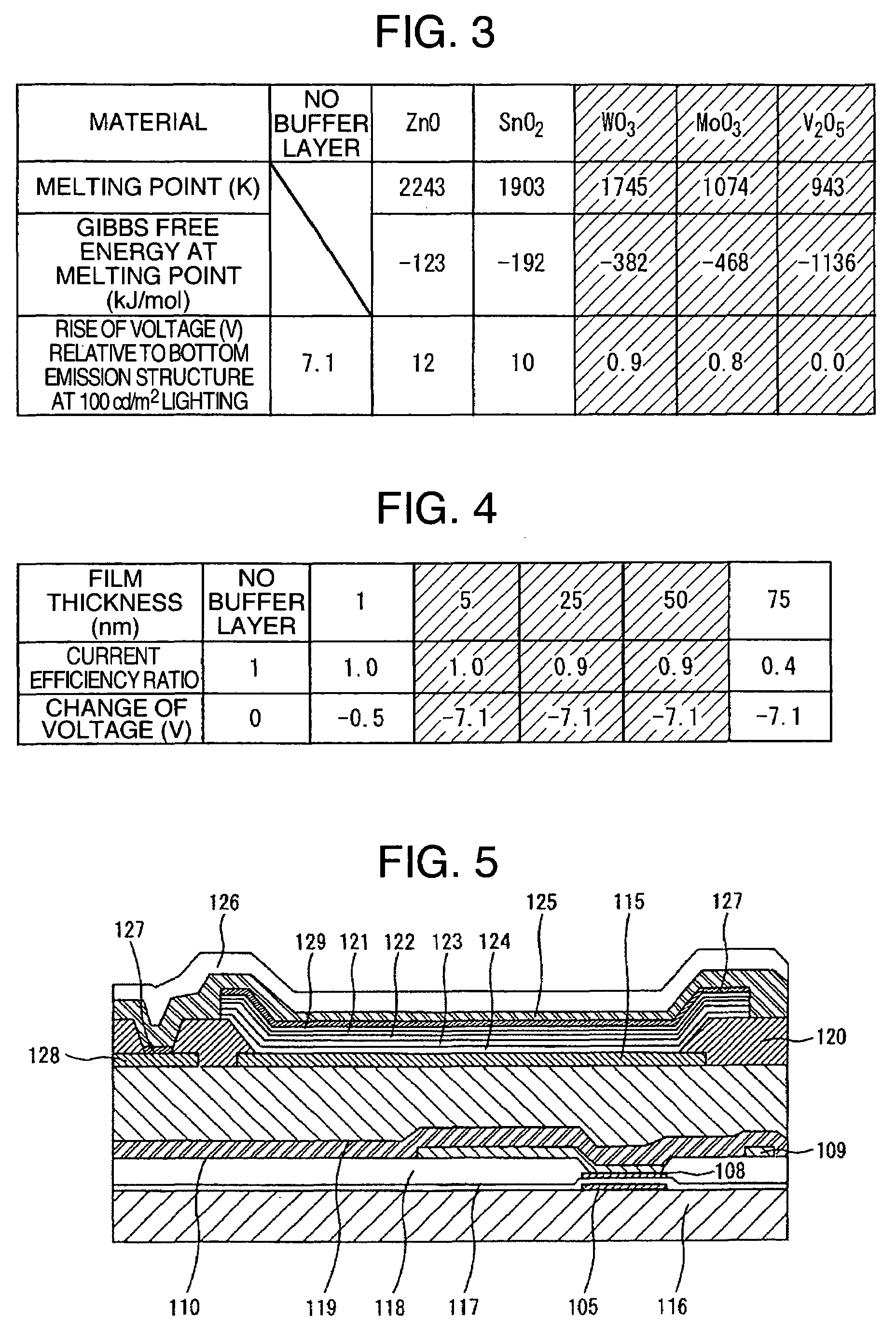
[0097]A film of vanadium oxide was formed as buffer layer 127 by EB deposition using a shadow mask for patterning. The film thickness was 1, 5, 25, 50 and 75 nm. A similar display device having no buffer layer was also made by way of comparison. The vanadium oxide film had a composition of V:O=1:2.45.
[0098]FIG. 4 shows the change of voltage and current efficiency ratio according to the buffer layer thickness at 100 cd / m2 light emission. The change of voltage shown here is the one relative to the device having no buffer layer. Current efficiency ratio is the ratio to the current efficiency of the device having no buffer layer which is supposed to be 1.
[0099]If the buffer layer thickness is less than 5 nm, oxidation of the organic film can not be ...
example 3
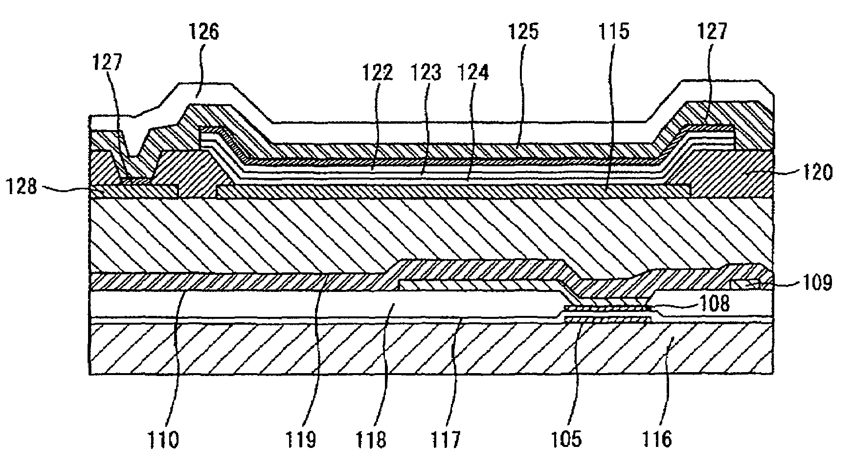
[0100]Still another example of the organic light-emitting display device according to the present invention will be explained. FIG. 5 is a sectional view of the organic light-emitting display device in the instant example of the present invention.
[0101]The organic light-emitting display device of this example is an active matrix type organic light-emitting display device comprising: a plurality of pixels; and a thin film transistor driving these pixels; wherein each of said pixels has an organic light-emitting element which comprises: an organic light-emitting layer; and an upper electrode and a lower electrode sandwiching the said organic light-emitting layer; wherein a light emitted from the organic light-emitting layer is taken out from the upper electrode side, said upper electrode is connected to an auxiliary electrode made of a low-resistance material, said organic light-emitting element has its constituent layers arranged in the order of lower electrode, organic light-emittin...
PUM
 Abstract
Description
Claims
Application Information