Probe card, semiconductor inspecting apparatus, and manufacturing method of semiconductor device

a manufacturing method and semiconductor technology, applied in the direction of individual semiconductor device testing, semiconductor/solid-state device testing/measurement, instruments, etc., can solve the problems of short-circuit between wires and foreign objects, material with lower dielectric constant damage, and contact resistance becoming unstabl

Inactive Publication Date: 2011-06-07
RENESAS ELECTRONICS CORP
View PDF22 Cites 21 Cited by
  • Summary
  • Abstract
  • Description
  • Claims
  • Application Information

AI Technical Summary

Benefits of technology

[0014]Since it is necessary to bring contact terminals for inspection in contact with fine electrode pads for inspection of a semiconductor element arranged at a narrow pitch with a high positional precision, and it is necessary to prevent occurrence of connection failure at a time of wire bonding using electrode pads or a time of forming bumps for connection at the subsequent steps, roughness of electrode pad faces caused by probing must be prevented as far as possible. Therefore, a probing trace is required to be made finer as far as possible.
[0015]In an inspecting apparatus which conducts probing perpendicularly to electrodes for inspection of a semiconductor element using the four-sided pyramid-shaped contact terminals shown in FIG. 30, a contact resistance value is stable, but when further narrow pitch configuration and higher speed electric signal are required in recent years, further improvement of a positional accuracy of a distal end of the contact terminal is required. In addition, material with low dielectric constant relatively weak in withstand load tends to be used as material for forming a circuit for high-speed transmission, and a further lower load probe is required in order to prevent damage to a semiconductor device at a time of probing.
[0016]An object of the present invention is to provide a probe card for semiconductor device inspection which allows probing inspection without damaging to an electrode pad to be contacted owing to low load and which has contact terminals with multi-point and high density configuration which can achieve contact with small probing trace and is excellent in transmission characteristic and stable in contact characteristic.
[0017]Another object of the present invention is to provide a probe card which can hold accuracy of a distal end of a contact terminal at a time of probing inspection in high level.
[0018]A still another object of the present invention is to provide a probe card for semiconductor device inspection using a probe sheet with reduced loss of high-speed transmission signal by realizing a high-speed transmission circuit with impedance matching.

Problems solved by technology

As a result, by rubbing an electrode by a contact terminal, shaving of electrode material occurs, which causes short-circuiting between wires and foreign matter occurrence.
By rubbing a probe against an electrode with applying load of about several hundreds mN or more to secure a contacting state, material with lower dielectric constant may be damaged.
Thus, when a method of using a bump formed at a portion of a wire by plating the portion of wiring as a probe as shown in FIGS. 27 to 29 is adopted, since a distal end portion of the bump becomes flat or hemispherical, it is difficult to remove oxide from material to be contacted such as an aluminum electrode or a solder electrode producing oxide on its material surface in a rubbing manner, so that contact resistance becomes unstable, where load at a time of contacting or rubbing must be set to about several hundreds mN or more.
However, excessive increase of load at a time of the contacting is problematic.
That is, since electrodes with high density, multi-pin and narrow pitch configuration are formed on a surface of a semiconductor element due to advance of denser integration of the semiconductor device, many active devices or fine wires are frequently formed just below the electrodes, and when contact pressure of a probe to electrodes at a time of an inspection of the semiconductor element is excessively large, the electrode(s), or the active device(s) and the wire(s) just below the electrode(s) may be damaged, so that it is necessary to conduct operation control at a time of probing carefully, which may result in lowering of throughput of inspection.
Since it is anticipated that variations occur in shapes of bumps or the like, further large contacting load is required as a whole in order to achieve full contact of a protrusion (bump) put in insufficient contact, which results in such a problem that excessive contact pressure acts partially.

Method used


Image

  • Probe card, semiconductor inspecting apparatus, and manufacturing method of semiconductor device
  • Probe card, semiconductor inspecting apparatus, and manufacturing method of semiconductor device
  • Probe card, semiconductor inspecting apparatus, and manufacturing method of semiconductor device

Examples


first embodiment

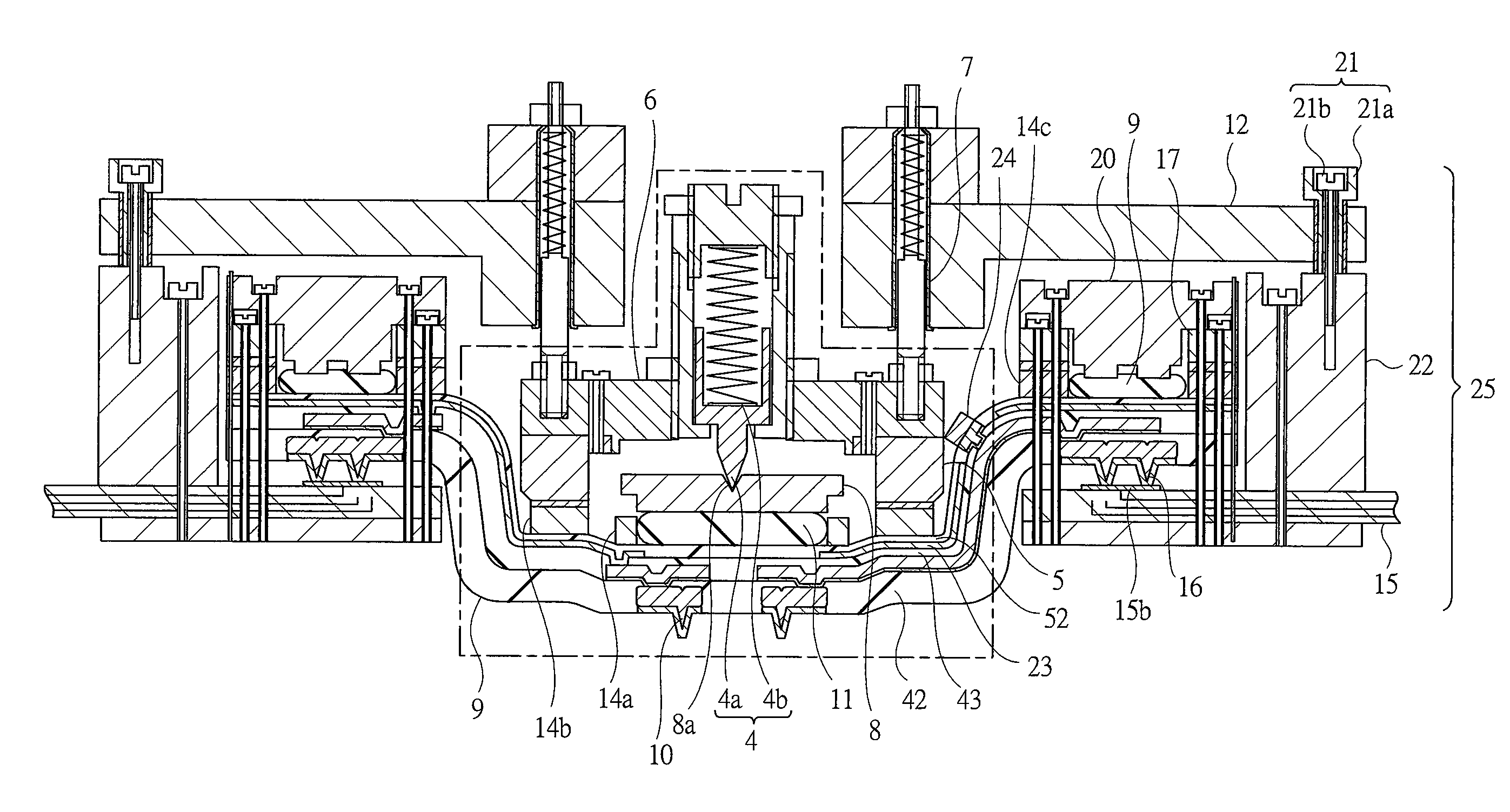
[0156]FIG. 2 is a cross sectional view showing a main portion of a probe card according to a first embodiment, FIG. 3 is a perspective view showing main parts shown in FIG. 2 in an exploded manner, and FIG. 4 a sectional view showing assembling of main parts of the probe card shown in FIG. 2 in an exploded manner. A probe card according to the first embodiment will be explained with reference to FIGS. 2 to 5.

[0157]The probe card according to the first embodiment includes a spring plunger 4, a frame 5, an intermediate plate 6, a plurality of guide pins 7, and the like.

[0158]The spring plunger (means for imparting a pressing force to a probe sheet center) 4 is fixed to a central portion of the intermediate plate 6 such that it is adjustable in its height direction, it has a protrusion portion 4a at its lower end to serve as a center pivot, and it is provided with a spring 4b imparting pressing force to a probe sheet 9 via a pushing piece 8 movable about a distal end of the protrusion ...

second embodiment

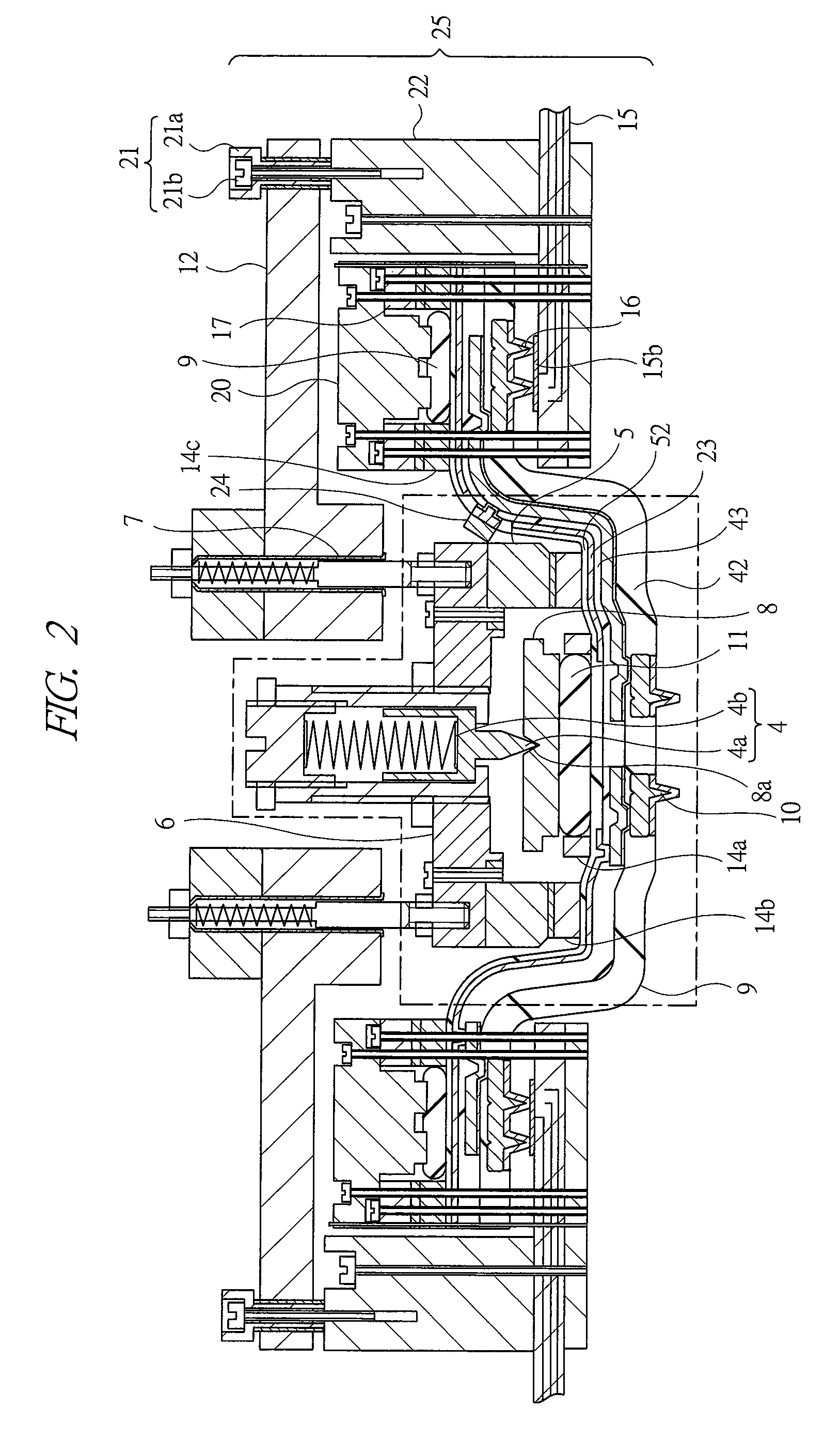
[0175]FIG. 7 is a cross sectional view showing a main portion of a probe card according to a second embodiment. In the first embodiment, the case that the ground wire 23 is formed on the probe sheet 9 and the chip capacitor 24 is attached thereon has been shown (see FIG. 2 and FIG. 6), but when a high-speed electric inspection signal is not required, as shown in FIG. 7, such a configuration that the ground wire 23, the chip capacitor 24, or the both may be omitted may be adopted.

[0176]In a configuration of a probe card explained below, such a configuration can be adopted depending on a speed of an inspection signal that the ground wire 23 or the chip capacitor 24 has been omitted like the above. The double screw 21 for fine adjustment of inclination (see FIG. 2) or the spacer 22a (see FIG. 6) can be used according to needs and it may be omitted, of course.

[0177]In FIG. 2 shown in the first embodiment, the example where the metal film 14a and the metal film 14b on a region correspond...

third embodiment

[0180]FIG. 8 is a cross sectional view showing a main portion of a probe card according to a third embodiment and FIG. 9 is a sectional view of a main portion showing the vicinity of a contact terminal 10 of the probe card according to the third embodiment in an enlarged manner. The probe card according to the third embodiment will be explained with reference to FIGS. 8 and 9.

[0181]In the probe sheet 9, when a connection electrode portion 10b on which individual contact terminals 10 are formed and a wire material 26 are connected to each other, via holes are utilized in the first embodiment, but, in the third embodiment, via holes are omitted and a wire material 26 is directly formed on the surface of the connection electrode portion 10b (see FIG. 9). The other configuration of the third embodiment is similar to those of the first embodiment.

[0182]According to a probe sheet structure 25c of the third embodiment with such a structure, since a structure where via holes are omitted is ...


PUM


Abstract

A frame bonded and fixed to a back face of a probe sheet so as to surround a group of pyramid-shaped or truncated pyramid-shaped contact terminals collectively formed at a central region portion of the probe sheet on a probing side thereof is protruded from a multi-layered wiring board, and pressing force is imparted to the frame and a pressing piece at a central portion by a plurality of guide pins having spring property so as to tilt finely.

Description

CROSS-REFERENCE TO RELATED APPLICATION[0001]The present application claims priority from Japanese Patent Application No. JP 2007-205953 filed on Aug. 7, 2007, the content of which is hereby incorporated by reference into this application.TECHNICAL FIELD OF THE INVENTION[0002]The present invention relates to a probe card, a semiconductor inspecting apparatus, and a manufacturing method of a semiconductor device, and in particular to an effective technique applied to a probe sheet formed in a similar technique to that used in manufacture of a semiconductor device, a probe card using the probe sheet, a semiconductor inspecting apparatus including the probe card, and a manufacturing step of a semiconductor device including an inspecting step conducted by the semiconductor inspecting apparatus.BACKGROUND OF THE INVENTION[0003]One example of flow of an inspecting step of manufacturing steps of a semiconductor device performed after formation of semiconductor element circuits on a semicond...

Claims


Application Information

Patent Timeline
Patent Type & Authority Patents(United States)
IPC IPC(8): G01R31/00
CPCG01R1/07342G01R31/2889G01R3/00G01R31/2875H01L22/00
Inventor KASUKABE, SUSUMUOKAMOTO, NAOKI
Owner RENESAS ELECTRONICS CORP
Why Eureka
Try Eureka