

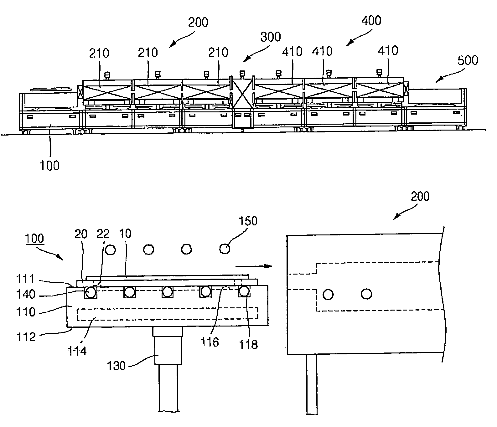
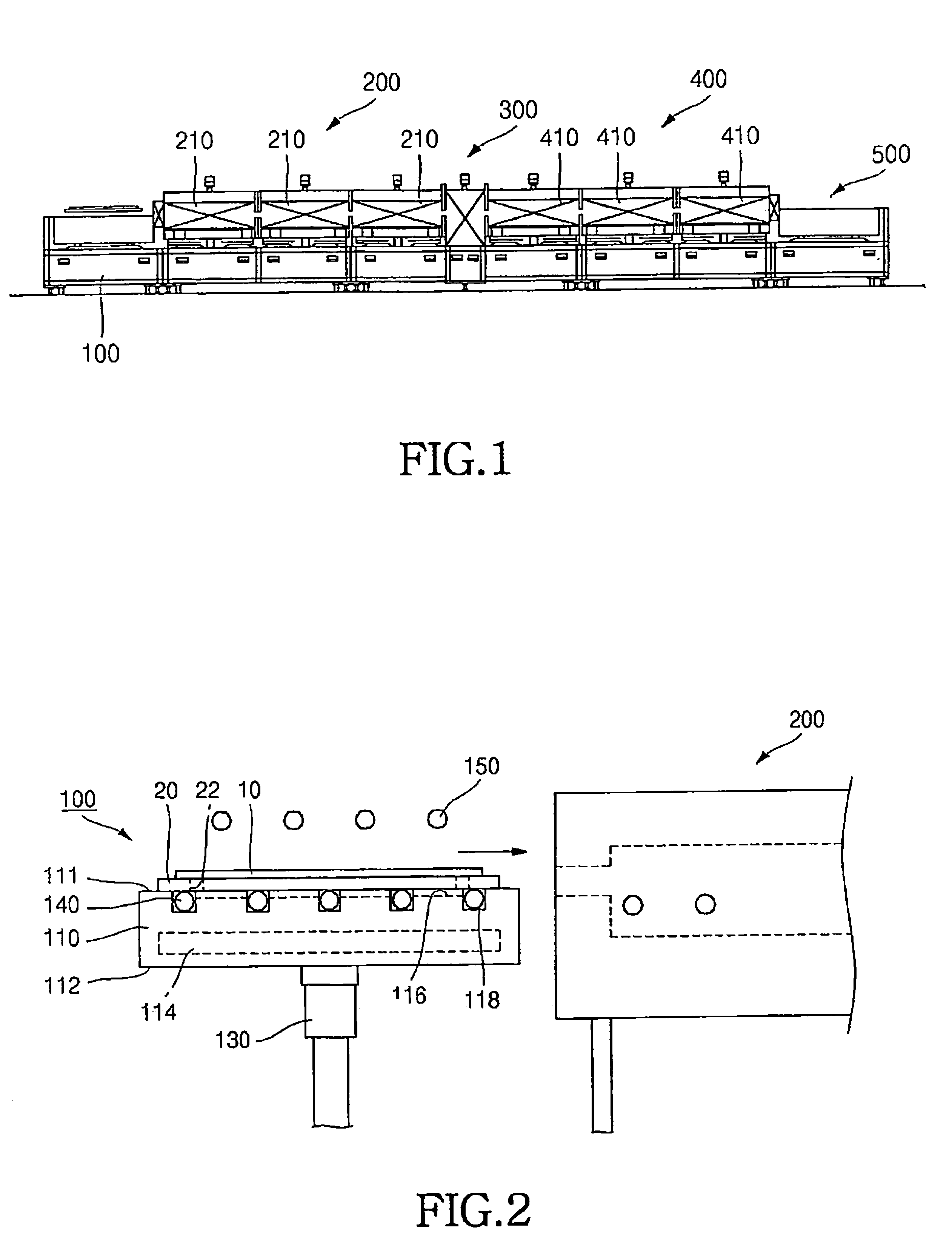
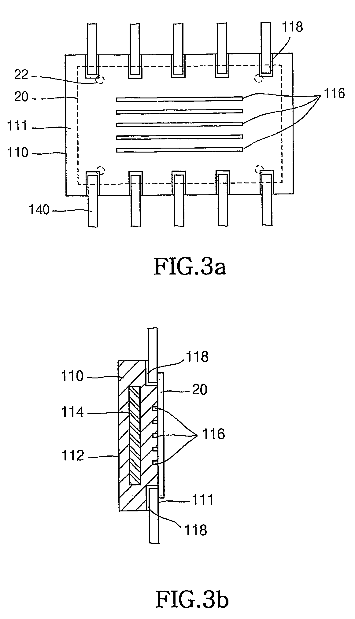
System for heat treatment of semiconductor device
a heat treatment system and semiconductor technology, applied in lighting and heating apparatus, electric/magnetic/electromagnetic heating, furnaces, etc., can solve the problems of lowering the driving characteristics of the semiconductor device, and increasing current leakage, so as to prevent deformation or damage of the semiconductor device caused by the local temperature difference in the semiconductor device, the effect of increasing the temperature of the semiconductor devi
- Summary
- Abstract
- Description
- Claims
- Application Information
AI Technical Summary
Benefits of technology
Problems solved by technology
Method used
Image

Examples
application example 1
[0161]According to application example 1, the heat treatment system of the present invention is used for the SPC process of the amorphous silicon thin film deposited on the semiconductor device, that is, the glass substrate.
[0162]FIG. 17 is a graph illustrating a UV slope, which represents the crystallization degree of the amorphous silicon thin film as a function of current of the induction coil. That is, FIG. 17 shows the crystallization degree of the amorphous silicon thin film as a function of current of the induction coil under the same heat treatment time for the glass substrate, wherein an X-axis represents the current of the induction coil and a Y-axis represents the UV curve. The crystallization degree of the amorphous silicon thin film according to a UV transmittance spectrum may be estimated based on the UV slope value, wherein a silicon thin film having high quality crystalline can be obtained as the UV slope value becomes high.
[0163]FIGS. 18a to 18d are graphs illustrat...
application example 2
[0166]According to application example 2, the heat treatment system of the present invention is used for the MILC process of the amorphous silicon thin film deposited on the semiconductor device, that is, the glass substrate.
[0167]FIG. 19 is a view illustrating a growing length of an MILC layer as a function of current of the induction coil after the MICL process has been finished.
[0168]After depositing the amorphous silicon thin film on the glass substrate through the chemical vapor deposition process, a metal element (Ni) is coated on a predetermined portion of the amorphous silicon thin film in order to perform the MILC process. Herein, the MILC process is performed in the same manner as the crystallization process of application example 1, except that the preheating temperature of the furnace is set to 600° C., which is lower than that of application example 1. At this time, the processing unit 300 performs the heat treatment process while adjusting current applied to the haloge...
application example 3
[0170]According to application example 3, the heat treatment system of the present invention is used for the dopant activation process to activate the dopant doped into the crystalline silicon thin film.
[0171]FIG. 20 is a graph illustrating the activation degree of the dopant as a function of the heating temperature and power of halogen lamps.
[0172]After depositing the amorphous silicon thin film on the glass substrate through the chemical vapor deposition process, the amorphous silicon thin film is crystallized into the poly-crystalline silicon thin film through the ELC process. Then, after depositing a silicon dioxide (SiO2) layer as an insulation layer, an n-type dopant is doped into the poly-crystalline silicon thin film by using doping equipment. According to application example 3, the dopant activation process is performed in the same manner as the crystallization process and the MILC process used in application examples 1 and 2, except that the preheating temperature of the f...
PUM
| Property | Measurement | Unit |
|---|---|---|
| width | aaaaa | aaaaa |
| temperature | aaaaa | aaaaa |
| thickness | aaaaa | aaaaa |
Abstract
Description
Claims
Application Information