Deep trench varactors

a technology of deep trenches and varactors, applied in the field of deep trenches varactors, can solve the problems of corresponding increase in thickness, degradation of device performance, and negatively affecting the performance of such mos varactors, and achieve the effect of minimal leakage current and high areal capacitance density

Inactive Publication Date: 2011-08-30
GLOBALFOUNDRIES US INC
View PDF18 Cites 7 Cited by
  • Summary
  • Abstract
  • Description
  • Claims
  • Application Information

AI Technical Summary

Problems solved by technology

With the scaling of the gate dielectric in semiconductor technology, however, performance of such MOS varactors is negatively impacted by leakage current through the node dielectric, which has the same thickness as the gate dielectric since both are formed at the same processing step and have identical composition and thickness.
While use of a thicker dielectric layer for the node dielectric could reduce leakage current through the prior art varactors, such changes will accompany degradation of device performance for field effect transistors that have a gate dielectric with a correspondingly increased thickness.
Further, such an approach negatively impacts the tunability of a varactor by decreasing the maximum capacitance in an accumulation mode.
While deep trench capacitors employing a separate thicker node dielectric with minimal leakage current and high areal capacitance density are also known in the art, such deep trench capacitors are linear capacitors having a constant capacitance, and do not provide any variability in capacitance.

Method used


Image

  • Deep trench varactors
  • Deep trench varactors
  • Deep trench varactors

Examples


first embodiment

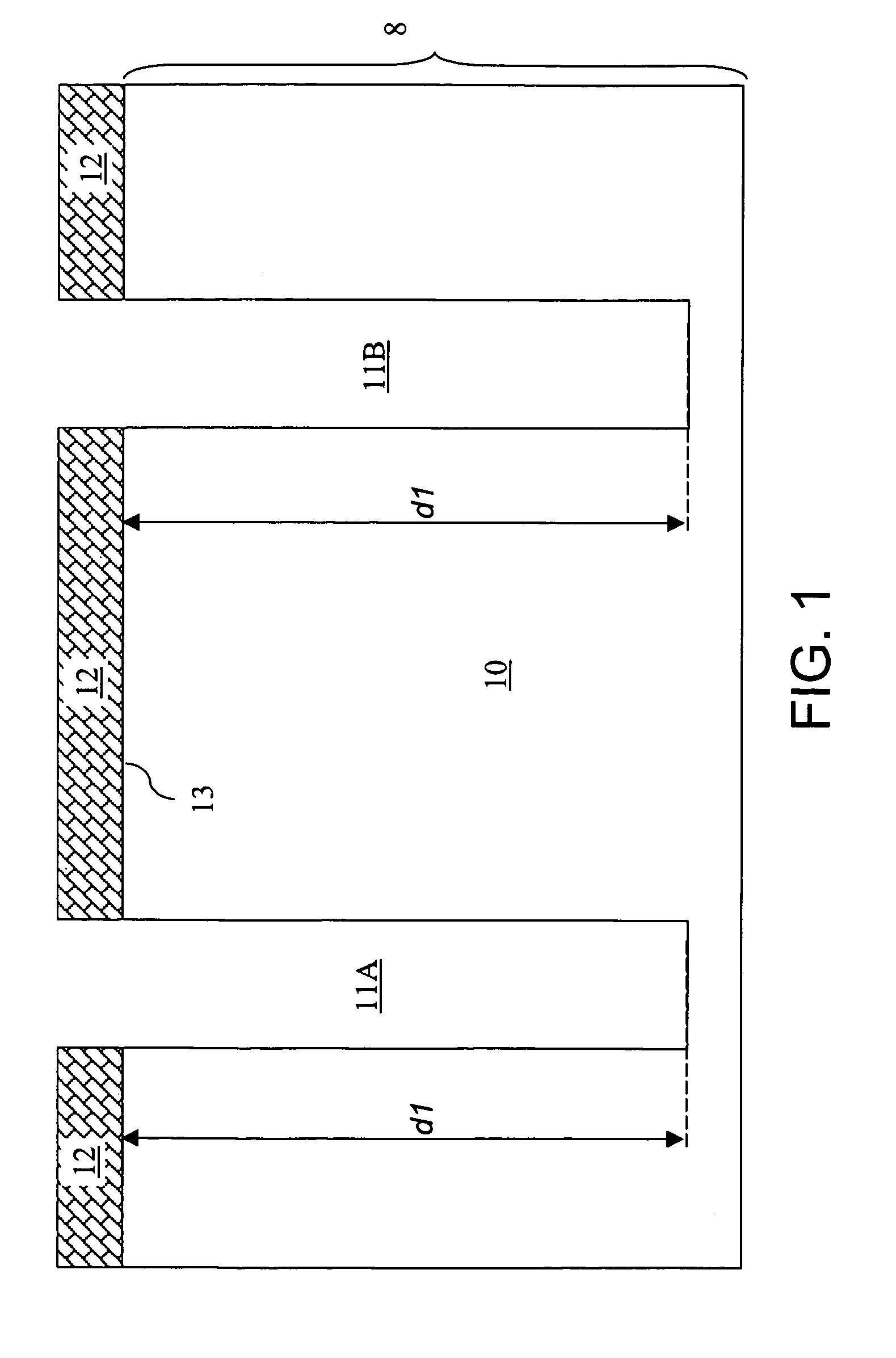
[0079]Referring to FIG. 1, a first exemplary semiconductor structure according to the present invention comprises a semiconductor substrate 8 containing a semiconductor region 10, a first deep trench 11A, and a second deep trench 11B. Preferably, the semiconductor region 10 comprises a single crystalline semiconductor material. The semiconductor material may be selected from, but is not limited to, silicon, germanium, silicon-germanium alloy, silicon carbon alloy, silicon-germanium-carbon alloy, gallium arsenide, indium arsenide, indium phosphide, III-V compound semiconductor materials, II-VI compound semiconductor materials, organic semiconductor materials, and other compound semiconductor materials. Typically, the semiconductor material comprises silicon. Preferably, the semiconductor substrate 8 is a single crystalline substrate in which the entirety of the semiconductor region 10 is epitaxially aligned single crystalline material. The semiconductor substrate 8 may be a bulk subs...

third embodiment

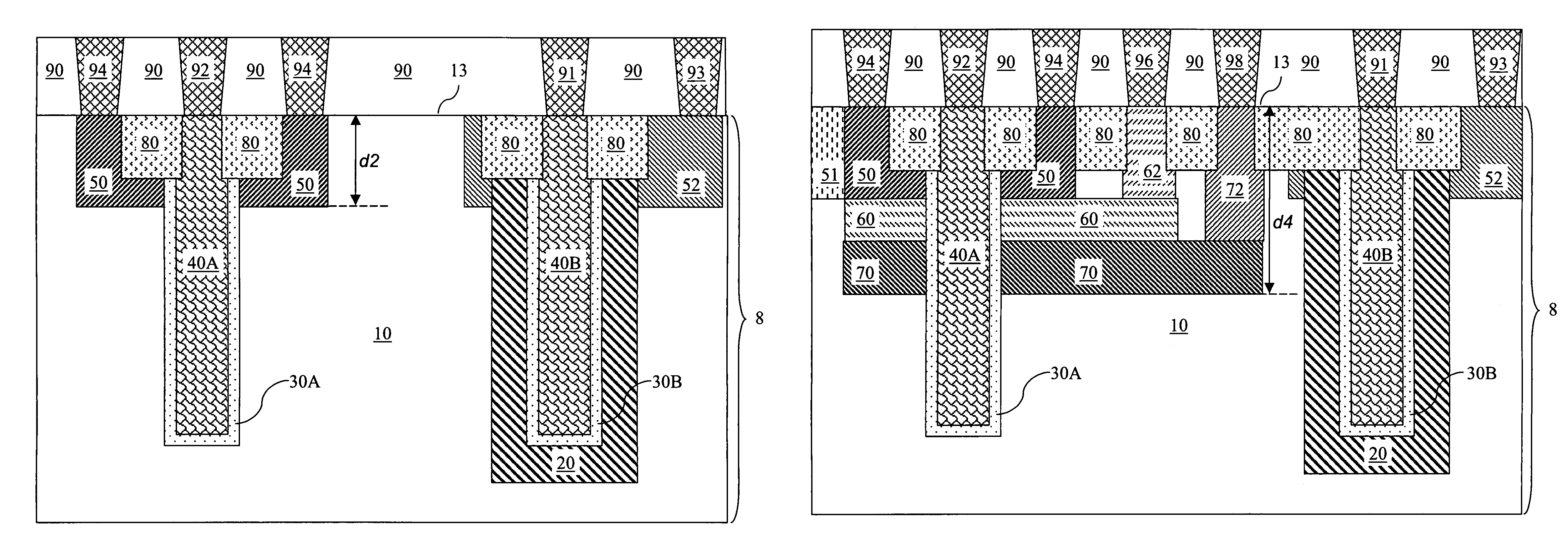
[0111]Referring to FIG. 11, a third exemplary semiconductor structure according to the present invention is derived from the first exemplary semiconductor structure by formation of a second doped well 60 and a first reachthrough 62 providing electrical contact to the second doped well 60. The second doped well 60 and the first reachthrough 62 are formed by masked ion implantation. The second doped well 60 is formed directly underneath the first doped well 50. The depth of the bottom surface of the second doped well 60, which is herein referred to as a third depth d3, is greater than the second depth d2 (See FIG. 7) and less than the first depth d1. The third depth d3 may be from about 200 nm to about 2,000 nm, and typically from about 400 nm to about 1,500 nm, although lesser and greater depths are also contemplated herein. The second doped well 60 and the first doped well 50 have different dopant concentrations or different doping conductivity types. The second doped well 60 has th...

fourth embodiment

[0117]Referring to FIG. 12, a fourth exemplary semiconductor structure according to the present invention is derived from the third exemplary semiconductor structure by formation of a third doped well 70 and a second reachthrough 72 providing electrical contact to the third doped well 60. The third doped well 70 and the second reachthrough 72 are formed by masked ion implantation. The third doped well 70 is formed directly underneath the second doped well 60. The depth of the bottom surface of the third doped well 70, which is herein referred to as a fourth depth d4, is greater than the third depth d3 (See FIG. 11) and less than the first depth d1. The fourth depth d4 may be from about 300 nm to about 2,000 nm, and typically from about 600 nm to about 2,000 nm, although lesser and greater depths are also contemplated herein. The third doped well 70 has a different dopant concentration or a different doping conductivity type than the first doped well 50. The third doped well 70 has a...


PUM


Abstract

A deep trench varactor structure compatible with a deep trench capacitor structure and methods of manufacturing the same are provided. A buried plate layer is formed on a second deep trench, while the first trench is protected from formation of any buried plate layer. The inside of the deep trenches is filled with a conductive material to form inner electrodes. At least one doped well is formed outside and abutting portions of the first deep trench and constitutes at least one outer varactor electrode. Multiple doped wells may be connected in parallel to provide a varactor having complex voltage dependency of capacitance. The buried plate layer and another doped well connected thereto constitute an outer electrode of a linear capacitor formed on the second deep trench.

Description

FIELD OF THE INVENTION[0001]The present invention relates to a semiconductor structure, and particularly to deep trench varactors compatible with deep trench linear capacitors and methods of manufacturing the same.BACKGROUND OF THE INVENTION[0002]A varactor is a semiconductor device having a voltage-sensitive capacitance. Frequently, the space-charge region and the accumulation at the surface of a semiconductor contacting an insulator are altered as a function of applied voltage to produce a bias-dependent capacitance.[0003]The variability of the capacitance in a varactor may be advantageously employed in various electronic circuits to provide useful functions in amplifiers, oscillators, and frequency synthesizers. For example, varactors may be used to construct voltage-controlled oscillators (VCO), which generates a tunable stable frequency without employing a circuit with multiple oscillators. U.S. Pat. No. 7,129,801 to Wu shows an exemplary use of a varactor in a VCO circuit. A V...

Claims


Application Information

Patent Timeline
Patent Type & Authority Patents(United States)
IPC IPC(8): H01L29/93
CPCH01L29/945H01L29/93H01L29/66181H01L27/0805H01L27/0808
Inventor COLLINS, DAVID S.RASSEL, ROBERT M.THOMPSON, ERIC
Owner GLOBALFOUNDRIES US INC
Why Eureka
Try Eureka