Deposition of doped copper seed layers having improved reliability

a technology of doped copper and seed layers, which is applied in the direction of semiconductor devices, semiconductor/solid-state device details, electrical apparatus, etc., can solve the problems of increasing the reliability of the device, reducing the electromigration performance, and short circuit, so as to improve the electromigration performance, reduce the resistance of lines, and reduce the effect of line resistance increas

Inactive Publication Date: 2011-09-13
NOVELLUS SYSTEMS
View PDF198 Cites 26 Cited by
  • Summary
  • Abstract
  • Description
  • Claims
  • Application Information

AI Technical Summary

Benefits of technology

[0006]The present invention provides improved methods of depositing copper seed layers in copper interconnect structure fabrication processes. The resulting structures have improved electromigration performance and reduced line resistance associated with the use of an alloy seed. According to various embodiments, the methods involve depositing a copper seed bilayer on a barrier layer in a recessed feature on a partially fabricated semiconductor substrate. The bilayer has a copper alloy seed layer and a pure copper seed layer, with the pure copper seed layer deposited on the copper alloy seed layer. The copper seed bilayers have reduced line resistance increase and provide better electromigration performance than conventional doped copper seed layers. Precise line resistance control can be achieved by tuning the bilayer thickness to meet the desired electromigration performance.

Problems solved by technology

An integration issue when using Cu as the primary conductor in devices is electromigration.
Extrusions can cause the Cu metal to extend past the Cu line into an adjacent Cu line, thereby causing a short circuit.
As the dimension of semiconductor devices continues to shrink, the reliability of the device, particularly the electromigration of copper interconnects, becomes more challenging.
This reduction of the electromigration performance is due to the increase of current density and decrease of the critical void dimension as the dimensions shrink.

Method used


Image

  • Deposition of doped copper seed layers having improved reliability
  • Deposition of doped copper seed layers having improved reliability
  • Deposition of doped copper seed layers having improved reliability

Examples


Embodiment Construction

[0017]In the following detailed description of the present invention, numerous specific embodiments are set forth in order to provide a thorough understanding of the invention. However, as will be apparent to those skilled in the art, the present invention may be practiced without these specific details or by using alternate elements or processes. In other instances well-known processes, procedures and components have not been described in detail so as not to unnecessarily obscure aspects of the present invention.

[0018]In this application, the term “wafer” will be used interchangeably with “partially fabricated integrated circuit.” One skilled in the art would understand that the term “partially fabricated integrated circuit” can refer to a silicon wafer during any of many stages of integrated circuit fabrication thereon. The term “substrate” is also used and includes wafers.

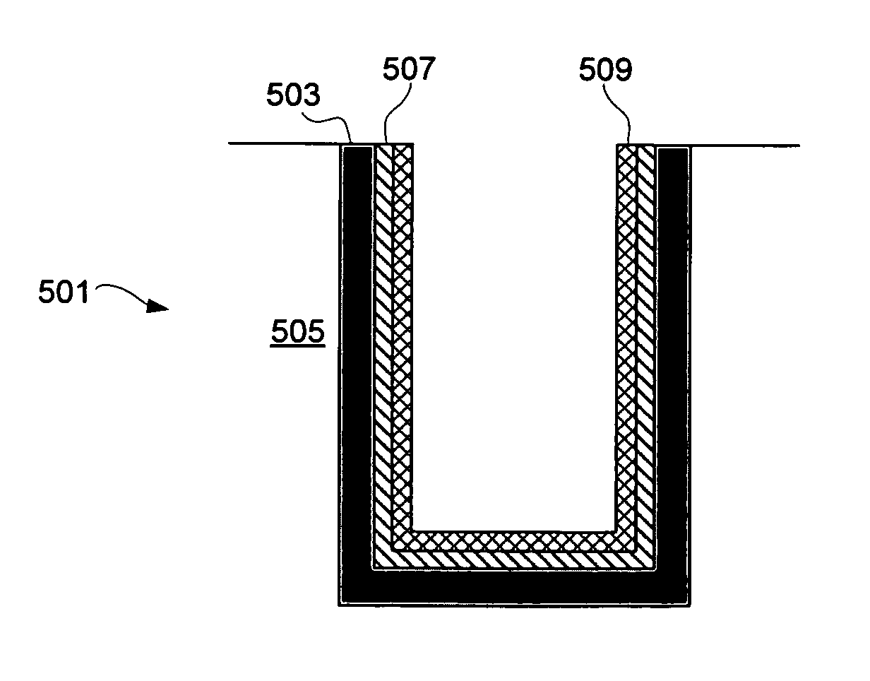
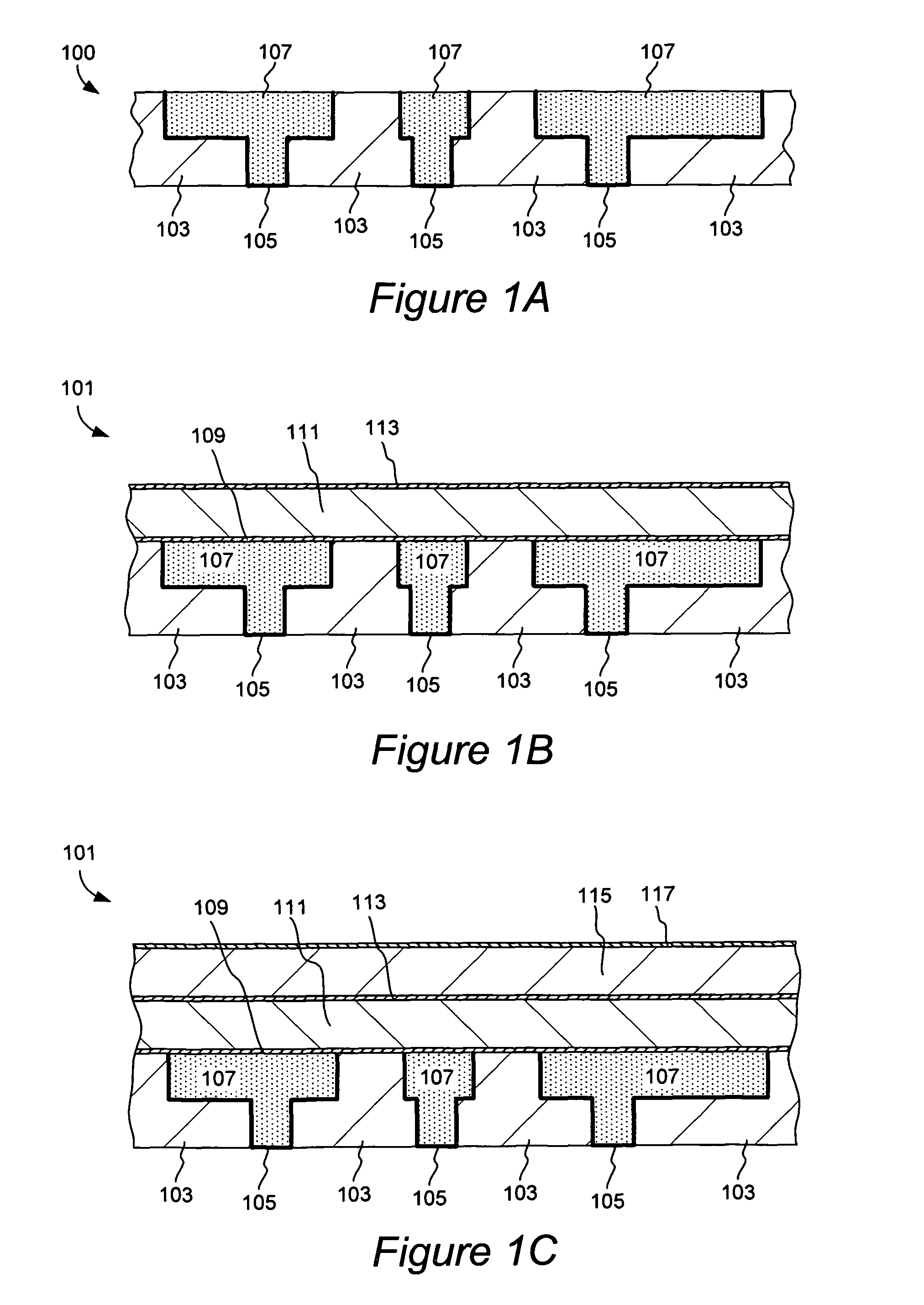
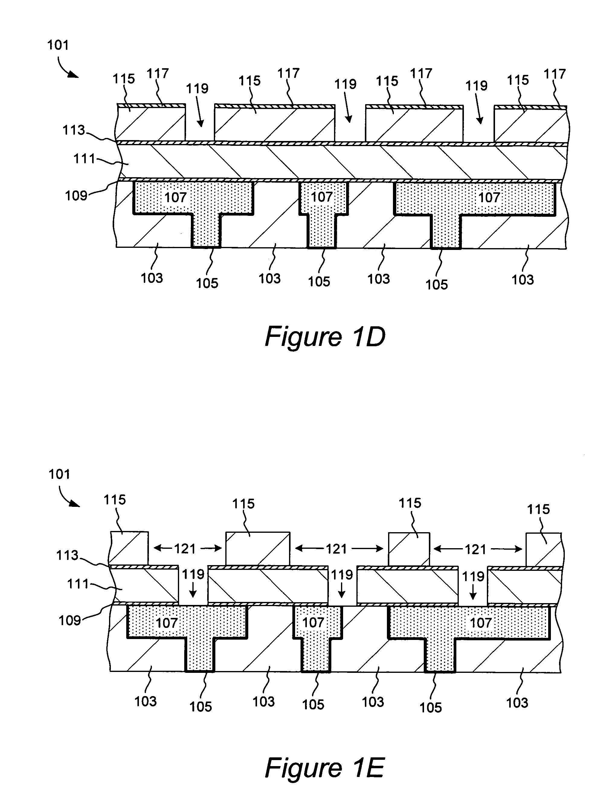
[0019]The invention finds particular use in damascene processing. FIGS. 1A-1H show cross sectional depictions...


PUM

PropertyMeasurementUnit
total thicknessaaaaaaaaaa
thicknessaaaaaaaaaa

Abstract

Improved methods of depositing copper seed layers in copper interconnect structure fabrication processes are provided. Also provided are the resulting structures, which have improved electromigration performance and reduced line resistance. According to various embodiments, the methods involve depositing a copper seed bilayer on a barrier layer in a recessed feature on a partially fabricated semiconductor substrate. The bilayer has a copper alloy seed layer and a pure copper seed layer, with the pure copper seed layer is deposited on the copper alloy seed layer. The copper seed bilayers have reduced line resistance increase and better electromigration performance than conventional doped copper seed layers. Precise line resistance control is achieved by tuning the bilayer thickness to meet the desired electromigration performance.

Description

FIELD OF THE INVENTION[0001]The present invention pertains to methods for forming a copper seed layer on a barrier layer of a partially fabricated integrated circuit.BACKGROUND OF THE INVENTION[0002]Damascene processing is a method for forming interconnections on integrated circuits that involves formation of inlaid metal lines in trenches and vias formed in a dielectric layer (inter-metal dielectric). The metal conductive lines are formed by an electroplating process. Because copper or other mobile conductive material provides the conductive paths of the integrated circuit, the underlying silicon devices must be protected from metal ions (e.g., Cu2+) that might otherwise diffuse or drift into the silicon. Suitable materials for diffusion barrier include tantalum, tantalum nitride, tungsten, titanium tungsten, titanium nitride, tungsten nitride, and the like.[0003]After the diffusion barrier is deposited and prior to electroplating, a seed layer of copper or other metal is typically...

Claims


Application Information

Patent Timeline
Patent Type & Authority Patents(United States)
IPC IPC(8): H01L21/4763
CPCH01L21/2855H01L21/76813H01L21/76865H01L21/76873H01L23/53238H01L21/76831H01L2221/1089H01L2924/0002
Inventor WU, HUI-JUNGJULIANO, DANIEL R.WU, WENDIXIT, GIRISH
Owner NOVELLUS SYSTEMS
Why Eureka
Try Eureka