Integrated circuit on high performance chip

a high-performance chip and integrated circuit technology, applied in the field of integrated circuits, can solve the problems of inability to easily meet the fabrication requirements of the active circuit, the nature of the layers and the treatment necessitated by the fabrication of the passive components, and the temperature is incompatible with the aluminum- or copper-based interconnection metal of the transistor, so as to reduce the effects of induced currents, reduce the effects of interference, and reduce the loss of induced currents

Inactive Publication Date: 2011-11-01
COMMISSARIAT A LENERGIE ATOMIQUE ET AUX ENERGIES ALTERNATIVES
View PDF323 Cites 82 Cited by
  • Summary
  • Abstract
  • Description
  • Claims
  • Application Information

AI Technical Summary

Benefits of technology

[0023]According to the invention, a second material may in particular be produced on a silicon substrate at a temperature higher than the maximum temperature to which the silicon substrate may be heated because of a first material already present on the wafer. The invention enables this by producing the second material separately from the silicon wafer on which it is to end up and then integrating the second material onto that wafer by layer transfer techniques. In the particular case of decoupling capacitors, the invention enables the dielectric material of the capacitor to be heated to temperatures enabling crystallization in the perovskite phase without any restriction being imposed by the underlying interconnection metal and without having recourse to a thermal protection barrier between the two materials.
[0024]The method of the invention also produces conveniently a structure for protecting the MEMS. This is because the MEMS being produced on the surface of the second substrate that is to be transferred onto the first substrate is this first substrate itself (in which an appropriate cavity has been formed beforehand) that serves as a protective structure for the MEMS after bonding the two substrates. This has the advantage that it economizes on the production of a cover as in the prior art.
[0025]According to particular features of the invention, dielectric insulation trenches intended to reduce electromagnetic interference between the various components of the future die are further produced during the production of the second substrate.
[0027]Certain other critical passive components are preferably produced in the vicinity of the face of the second substrate opposite the bonding face after said bonding of the two substrates. In the case of inductors, this has the advantage of considerably reducing the effects of the induced currents (energy losses, interference suffered by the active components, etc.), even if the second substrate is conductive, since this places the inductors far from the first substrate.
[0028]To reduce further the losses caused by induced currents and to improve the quality factors of the inductors, according to particular features, the inductors will be produced on top of inductive insulation trenches previously formed in the second substrate. A second aspect of the invention also relates to different dies containing integrated circuits.

Problems solved by technology

However, this monolithic integration causes a certain number of technological difficulties.
First, the nature of the layers and the treatments necessitated by the fabrication of the passive components are not always readily compatible with fabrication on the active circuits.
The perovskite crystalline phase is usually obtained at temperatures from 600° C. to 700° C. However, these temperatures are incompatible with the aluminum- or copper-based interconnection metal of the transistors.
Although certain prior art low-temperature processes use a perovskite (see for example the paper by D. Liu et al. entitled “Integrated Thin Film Capacitor Arrays”, International Conference on High Density Packaging and MCMs, 1999), they in fact relate to a phase in which the perovskite is not pure or is of mediocre structural or microstructural quality, which means that the dielectric constant is very much lower than that of the same material when annealed at a higher temperature.
The standard methods mentioned hereinabove therefore do not really exploit the advantages of perovskites, because the maximum authorized temperature decreases progressively as and when the process steps are carried out, and the main difficulty results from the fact that the placement of a “hot” process material (the dielectric) occurs after that of a “cold” process material (the interconnection metal).
This method is difficult to control, however, because the protective layer remains on the wafer.
The protective layer therefore cannot be very thick (it is usually less than 2 μm thick), and it may affect the electrical performance of the devices.
The temperature difference between the interconnection metal and the dielectric is therefore limited; in other words, the temperature to which the dielectric may be subjected is limited.
Moreover, the stack is subjected to a high thermal gradient during this operation, which can generate a surface temperature that is too high or cause non-homogeneous crystallization of the dielectric or deterioration of materials, such as microcracks, as a result of thermal expansion.
These methods have certain drawbacks, however: wires cannot be used to make short connections between capacitor and transistors, and microball connections may be produced on top of a circuit only once; if the capacitors are made of this material, it is no longer possible to add other functions such as switches or surface wave filters, for example.
Because of this temperature limit, these standard methods are greatly limited in terms of the type of material and the dielectric constants that can be achieved.
The required capacitance values are therefore obtained by producing capacitors occupying a large area, which limits the integration possibilities and adds to the cost of the die because of the increased area that is occupied on the silicon wafer.
However, apart from the difficulty of producing uniform dielectric layers in the trenches, the use of capacitor arrays in trenches makes planar integration of passive components with active components difficult.
More generally, a second difficulty arising from the monolithic integration of passive components or MEMS with transistors is that it is not possible to exploit the vertical dimension to improve the characteristics or the compactness of the passive components.
A third difficulty to which the monolithic integration of passive components or MEMS with transistors gives rise is that the type of substrate used for the active circuits disturbs the characteristics of the passive components.
The currents induced in these substrates by the inductors or conductive lines cause high losses and thereby reduce the quality factors of these structures (high inductance, high resonant frequency, low stray capacitance).
However, these various techniques are complex to use, may compromise the robustness of the integrated circuit and make the placement of active components difficult.
Finally, a difficulty raised specifically by the monolithic integration of MEMS with transistors is that it is necessary to add a cover to protect the mechanical components, without interfering with their operation.
This technology is relatively costly because it is necessary to add to the cost of the supplementary substrate the cost of bonding, the cost of thinning and the cost of local etching to obtain access to the output electrical contacts on the surface of the circuit, and all of this is needed only to provide protection by means of a cover.

Method used


Image

  • Integrated circuit on high performance chip
  • Integrated circuit on high performance chip
  • Integrated circuit on high performance chip

Examples


Embodiment Construction

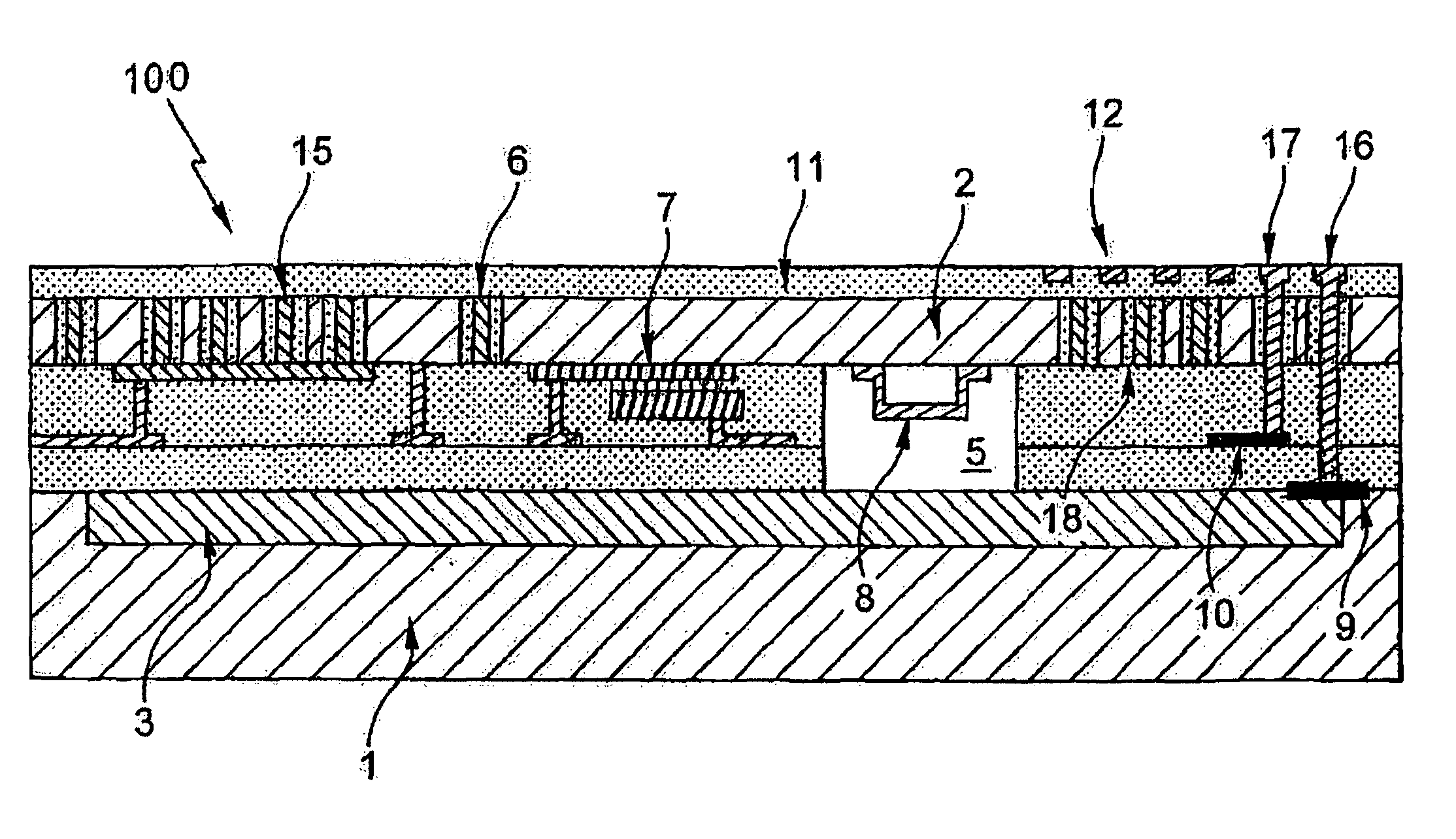
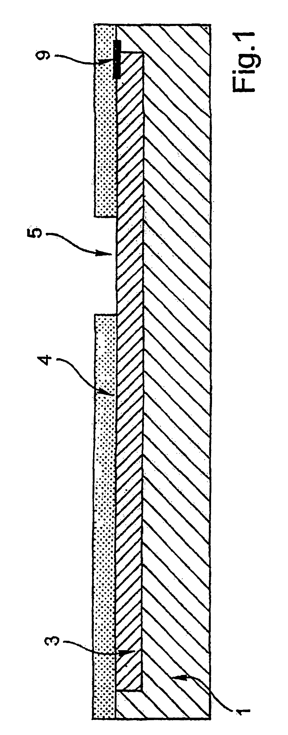
[0040]FIG. 1 shows a “first” substrate 1 consisting of a wafer of silicon or any other type III-V semiconductor material. The method of the invention begins with the preparation of two substrates 1 and 2 in either order or simultaneously. This first substrate 1 contains active components 3 that have been integrated by any technique known in the art (for example the CMOS or BICMOS technique) and metal interconnections (not shown).

[0041]In this embodiment, a thick layer 4 of insulation, for example SiO2, is deposited and, where appropriate, etched locally (forming cavities 5) in vertical alignment with any Microelectromechanical Systems (MEMS) components on the second substrate. Finally, metallization areas 9 are produced that are subsequently connected to other portions of the die (see below).

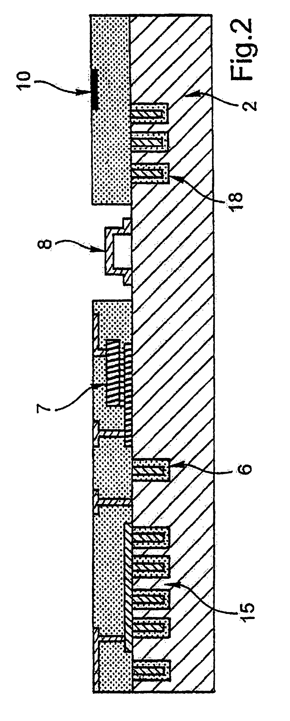
[0042]FIG. 2 represents a wafer forming a “second” substrate 2. In this embodiment, the second substrate 2 has been formed with: dielectric insulating trenches 6, capacitors 7 with a very high d...


PUM


Abstract

A method of fabricating a die containing an integrated circuit, including active components and passive components, includes producing a first substrate containing at least one active component of active components and a second substrate containing critical components of the passive components, such as perovskites or MEMS, and bonding the two substrates by a layer transfer. The method provides an improved monolithic integration of devices such as MEMS with transistors.

Description

RELATED APPLICATIONS[0001]This application claims priority from French Patent Application No. 0307617 filed Jun. 24, 2003, which is incorporated by reference herein.BACKGROUND[0002]The present invention relates to the field of integrated circuits, and in particular to that of passive components integrated on die.[0003]In the field of integrated circuits, there is an increasing requirement: to reduce the size taken up by the components, to reduce the fabrication costs, and to introduce new functions.[0004]To achieve these objectives, it is necessary to integrate collectively onto the same analog or digital integrated circuit die an increasing number of components that were previously fabricated separately. There are essentially three categories of such components: circuits called “active” (transistors), components called “passive” (resistors, capacitors, inductors), and, finally, micro-electro-mechanical systems (MEMS) (acoustic filters, radio-frequency switches, variable capacitors)...

Claims


Application Information

Patent Timeline
Patent Type & Authority Patents(United States)
IPC IPC(8): H01L21/30H01L27/08H01L29/06H01L21/46H01L21/02B81B7/00B81B7/02H01L21/20H01L21/822H01L21/98H01L25/16H01L27/06
CPCB81C1/00253H01L21/2007H01L21/8221H01L25/50H01L27/0688H01L28/10H01L25/16H01L2924/0002H01L2924/00
Inventor JOLY, JEAN-PIERREULMER, LAURENTPARAT, GUY
Owner COMMISSARIAT A LENERGIE ATOMIQUE ET AUX ENERGIES ALTERNATIVES
Why Eureka
Try Eureka