Method and system for near-field spectroscopy using targeted deposition of nanoparticles
a nanoparticle and near-field spectroscopy technology, applied in the direction of optical radiation measurement, instruments, spectrometry/spectrophotometry/monochromators, etc., can solve the problem that none of the known methods and systems provide all, and achieve the effects of short working distance optics, less complex, and fast optics
- Summary
- Abstract
- Description
- Claims
- Application Information
AI Technical Summary
Benefits of technology
Problems solved by technology
Method used
Image
Examples
example 1
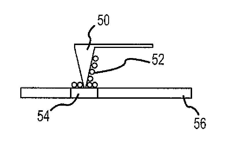
[0039]The first test sample was a thin film molecular layer of trans-1,2 bis-(4-pyridyl)ethylene (BPE) (Sigma-Aldrich) coating a quartz slide. The BPE film was cast from a dilute methanol solution using a droplet evaporation procedure developed for testing SERS substrates. The film could not be detected using conventional Raman scattering and was estimated to be approximately one to two molecular layers based on the grazing angle infrared reflectance spectrum. A gold nanoparticle solution (40 or 60 nm (nanometer), colloidal gold solution, obtained from Ted Pella of Redding, Calif.) was collected on a silicon AFM tip-cantilever and then deposited on the surface of the sample. The collection was made by engaging the AFM tip in contact mode to a drop of colloidal solution that was evaporated to approximately 50% of its original volume. The collection time was approximately one (1) second (s). Deposition was made immediately after collection of the gold nanoparticle solution by engaging...
example 2
[0043]Localized SEIRA was tested using 60 nm (nanometer) colloidal gold similarly deposited from the AFM tip onto a silicone (DC200 polydimethyl siloxane, obtained from Dow Corning of Midland, Mich.) coated substrate. The film was cast from a dilute dichloromethane solution onto a polished silicon wafer. The measurement was made using a Varian / Digilab FTS 6000 Fourier transform infrared (FTIR) microscope with a UMA 600 microscope. The FTIR microscope was equipped with a liquid nitrogen cooled, narrow band, mercury cadmium telluride detector. The nanoparticle area was imaged by AFM after deposition. The location was registered by scribing or marking on the silicon substrate for the FTIR microscope. The far field illuminated area was 20×20 micron as set by the FTIR microscope aperture mask.
[0044]A similar result was demonstrated for SEIRA using 60 nm (nanometer) diameter gold nanoparticles deposited onto a thin silicone coated silicon wafer. FIG. 12 shows FTIR (Fourier transform infra...
PUM
| Property | Measurement | Unit |
|---|---|---|
| grain diameters | aaaaa | aaaaa |
| grain diameters | aaaaa | aaaaa |
| grain size | aaaaa | aaaaa |
Abstract
Description
Claims
Application Information


