Method and system for near-field spectroscopy using targeted deposition of nanoparticles

a nanoparticle and near-field spectroscopy technology, applied in the direction of optical radiation measurement, instruments, spectrometry/spectrophotometry/monochromators, etc., can solve the problem that none of the known methods and systems provide all, and achieve the effects of short working distance optics, less complex, and fast optics

Inactive Publication Date: 2009-10-01
CALIFORNIA INST OF TECH
View PDF15 Cites 9 Cited by
  • Summary
  • Abstract
  • Description
  • Claims
  • Application Information

AI Technical Summary

Benefits of technology

[0008]This need for a method and system for near-field spectroscopy using targeted deposition of nanoparticles is satisfied. None of the known methods and systems provide all of the numerous advantages discussed herein. Unlike known methods and systems, embodiments of the method and system of the disclosure may provide one or more of the following advantages: the method and system provide for apertureless near-field optical spectroscopy with an atomic force microscope (AFM); the method and system do not require optical integration with the AFM tip and enable the use of fast, short working distance optics; the method and system provide for directed deposition of nanoparticles using a modified dip pen nanolithography (DPN) method that enables spectrochemical analysis with a resolution below the diffraction limit; the method and system allow the region of surface enhanced spectroscopy to be selected and focused by the arrangement of nanoparticles on the sample surface; the method and system provide for nanoparticle arrangement which determines the area of enhancement and the tuning of the plasmon resonance; the method and system do not require complex integration of a probe microscope with the spectrometer or fabrication of specialized tips; the method and system provide for near-field optical enhancement using targeted deposition of nanoparticles that may be applied to Raman, infrared or fluorescence spectroscopy; the method and system are flexible, fast, less complex, provide increased sensitivity, selectivity and spatial resolution, and provide greater surface enhancement and greater enhanced signals; the method and system provide an efficient means to obtain chemical information from a target sample material; and the method and system can be used with surface enhanced spectroscopy, such as surface enhanced Raman scattering (SERS), surface enhanced infrared absorption (SEIRA), surface enhanced fluorescence, fluorescence and infrared absorption through plasmon and phonon mediated mechanisms, and other suitable surface enhanced spectroscopy methods and techniques.
[0010]In another embodiment of the method there is provided a method for analyzing a sample material using surface enhanced Raman scattering spectroscopy. The method comprises the steps of imaging the sample material with an atomic force microscope (AFM) to select an area of interest for analysis, depositing metal nanoparticles onto the area of interest with an AFM tip, illuminating the deposited nanoparticles with a Raman excitation laser, disengaging the AFM tip and acquiring a localized surface enhanced spectrum, and using the AFM tip to modulate the Raman excitation laser above the deposited nanoparticles to obtain improved sensitivity data and higher spatial resolution data from the sample material.

Problems solved by technology

None of the known methods and systems provide all of the numerous advantages discussed herein.

Method used


Image

  • Method and system for near-field spectroscopy using targeted deposition of nanoparticles
  • Method and system for near-field spectroscopy using targeted deposition of nanoparticles
  • Method and system for near-field spectroscopy using targeted deposition of nanoparticles

Examples


example 1

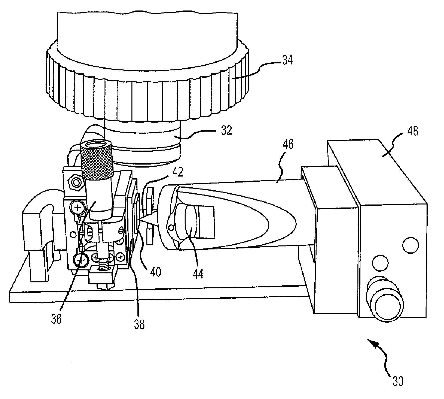
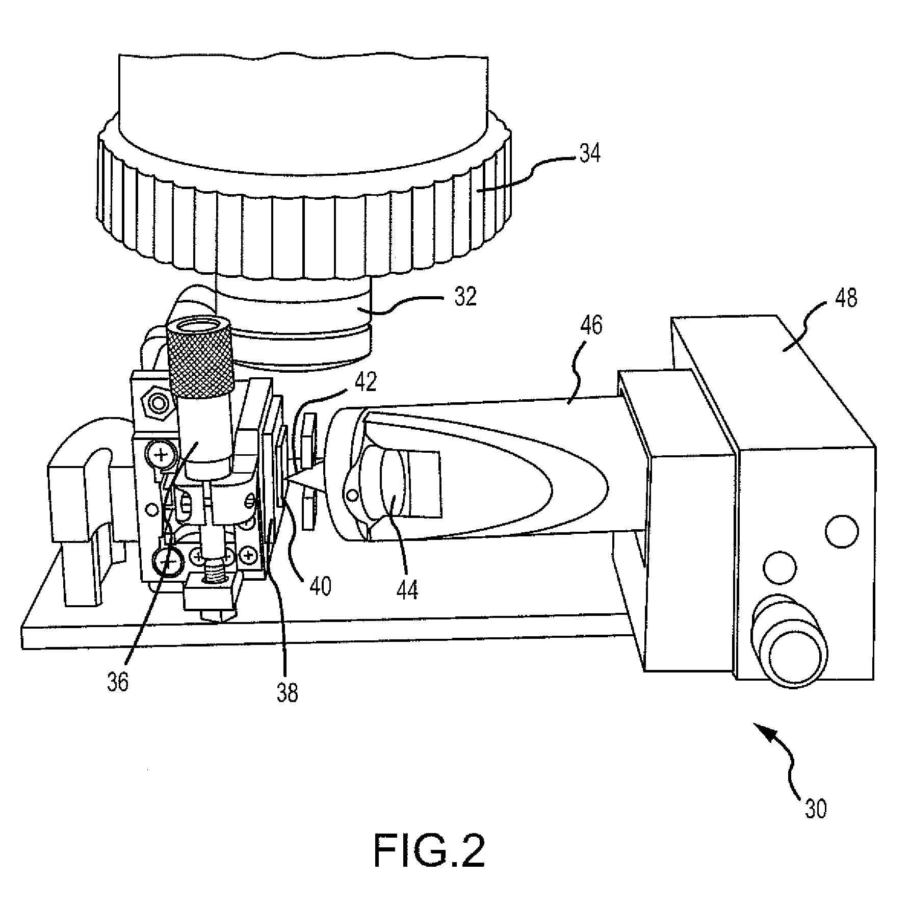
[0039]The first test sample was a thin film molecular layer of trans-1,2 bis-(4-pyridyl)ethylene (BPE) (Sigma-Aldrich) coating a quartz slide. The BPE film was cast from a dilute methanol solution using a droplet evaporation procedure developed for testing SERS substrates. The film could not be detected using conventional Raman scattering and was estimated to be approximately one to two molecular layers based on the grazing angle infrared reflectance spectrum. A gold nanoparticle solution (40 or 60 nm (nanometer), colloidal gold solution, obtained from Ted Pella of Redding, Calif.) was collected on a silicon AFM tip-cantilever and then deposited on the surface of the sample. The collection was made by engaging the AFM tip in contact mode to a drop of colloidal solution that was evaporated to approximately 50% of its original volume. The collection time was approximately one (1) second (s). Deposition was made immediately after collection of the gold nanoparticle solution by engaging...

example 2

[0043]Localized SEIRA was tested using 60 nm (nanometer) colloidal gold similarly deposited from the AFM tip onto a silicone (DC200 polydimethyl siloxane, obtained from Dow Corning of Midland, Mich.) coated substrate. The film was cast from a dilute dichloromethane solution onto a polished silicon wafer. The measurement was made using a Varian / Digilab FTS 6000 Fourier transform infrared (FTIR) microscope with a UMA 600 microscope. The FTIR microscope was equipped with a liquid nitrogen cooled, narrow band, mercury cadmium telluride detector. The nanoparticle area was imaged by AFM after deposition. The location was registered by scribing or marking on the silicon substrate for the FTIR microscope. The far field illuminated area was 20×20 micron as set by the FTIR microscope aperture mask.

[0044]A similar result was demonstrated for SEIRA using 60 nm (nanometer) diameter gold nanoparticles deposited onto a thin silicone coated silicon wafer. FIG. 12 shows FTIR (Fourier transform infra...


PUM

PropertyMeasurementUnit
grain diametersaaaaaaaaaa
grain sizeaaaaaaaaaa

Abstract

There is provided in one embodiment of the invention a method for analyzing a sample material using surface enhanced spectroscopy. The method comprises the steps of imaging the sample material with an atomic force microscope (AFM) to select an area of interest for analysis, depositing nanoparticles onto the area of interest with an AFM tip, illuminating the deposited nanoparticles with a spectrometer excitation beam, and disengaging the AFM tip and acquiring a localized surface enhanced spectrum. The method may further comprise the step of using the AFM tip to modulate the spectrometer excitation beam above the deposited nanoparticles to obtain improved sensitivity data and higher spatial resolution data from the sample material. The invention further comprises in one embodiment a system for analyzing a sample material using surface enhanced spectroscopy.

Description

CROSS-REFERENCE TO RELATED APPLICATION[0001]This application is related to and claims the benefit of priority under 35 U.S.C. Section 120 to U.S. Provisional Patent Application Ser. No. 61 / 005,069, filed Nov. 30, 2007, which is incorporated herein by reference in its entirety.GOVERNMENT INTERESTS[0002]The invention described herein was made in the performance of work under a NASA contract, and is subject to the provisions of Public Law 96-517 (35 U.S.C. 202) in which the Contractor has elected to retain title.BACKGROUND OF THE INVENTION[0003]a. Field of the Invention[0004]The invention relates to a method and system for near-field spectroscopy using targeted deposition of nanoparticles. In particular, the invention relates to a method and system for near-field spectroscopy using targeted surface enhanced Raman scattering (SERS) and surface enhanced infrared absorption (SEIRA) localized on deposited nanoparticles from an atomic force microscope (AFM) tip.[0005]b. Background Art[0006]...

Claims


Application Information

Patent Timeline
Patent Type & Authority Applications(United States)
IPC IPC(8): G12B21/06G01J3/44G01Q60/00
CPCB82Y15/00B82Y35/00G01J3/44G01Q60/06G01N21/658G01Q30/02G01N21/648
Inventor ANDERSON, MARK S.
Owner CALIFORNIA INST OF TECH
Why Eureka
Try Eureka