Methods and apparatus for the manufacture of microstructures

a microstructure and manufacturing method technology, applied in the direction of instruments, coatings, photographic processes, etc., can solve the problems of low cost, low cost, low cost of microstructures, and difficult mixing and matching manufacturing processes cost-effectively, so as to reduce processing errors, parasitic capacitance and leakage current, the effect of minimising contact overlap

Inactive Publication Date: 2012-02-28
3T TECH
View PDF14 Cites 10 Cited by
  • Summary
  • Abstract
  • Description
  • Claims
  • Application Information

AI Technical Summary

Benefits of technology

[0024]At least one of the masks may comprise a plurality of layers. One such layer may be reflective, preferably a layer between an adhesive layer and the masking film. This means that the adhesive layer is etched by the reflected laser light making peel-off easier Preferably the method comprises applying a reflective layer to the substrate. Such a mask may be applied to the substrate such that the reflective layer is the closest layer of the mask to the substrate and / or on the opposite side of the substrate to the mask. The method may comprise controlling a profile of the mask using the reflective layer, preferably through controlling the angle of reflection. The mask may have a predetermined layer thickness. Preferably the layers are bonded by adhesive. This aspect of the invention is to be able to etch the rear surface of the masking film from a reflective surface that is on the other surface of the transparent (to a substantial portion of the laser wavelength) substrate material. In this instance the masking film or film stack may be applied to the upper (top) surface of the substrate material and a second masking film may be applied to the lower (bottom) surface of the substrate material forming a sandwich structure. The lower surface mask may be so manufactured as to provide on, or in, the surface of the masking film closest to the bottom surface of the substrate a surface feature that causes an incoming parallel beam of laser light to be reflected at a controlled angle substantially in the direction of the incoming laser light (focussed beam). This reflected light may be of sufficient energy density so as to travel back along through the substrate material at the angle defined by the reflecting surface structure where it interacts with the surface preferably the lower surface of the surface in contact with the substrate of the upper masking structure so as to cause a volume of the masking film to be disrupted preferably by bond scission and preferably to be expelled under a pressure gradient into the space created by the initial laser etching of a feature into the upper masking structure. This may create a controlled geometry undercut that would ease peelable removal of the masking film structure preferably even with substantially conformal coating deposits.
[0099]This manufacturing process enables the use of a wide range of liquid, vapour, and solid particle processes to provide a very wide range of materials that permits the construction of all-inorganic, all-organic or hybridised inorganic-organic devices even mixing liquid, vapour and solid particle processes in one manufacturing sequence.

Problems solved by technology

However, there are disadvantages with many current fabrication processes.
In particular, it is difficult to manufacture low cost, relatively simple, microstructures cost effectively.
The need for economies of scale also means that it is difficult to mix and match manufacturing processes cost-effectively.
Present methods are particularly disadvantageous when it comes to the manufacture of flexible micro-structures, or the manufacture of micro-structures on a flexible substrate, such as in the manufacture of flexible displays.
The films which make up the multi-layer structure may break or become degraded (with respect to operational lifetime and performance and storage life) if over-flexed.

Method used


Image

  • Methods and apparatus for the manufacture of microstructures
  • Methods and apparatus for the manufacture of microstructures
  • Methods and apparatus for the manufacture of microstructures

Examples


an embodiment

of a Fabrication Process

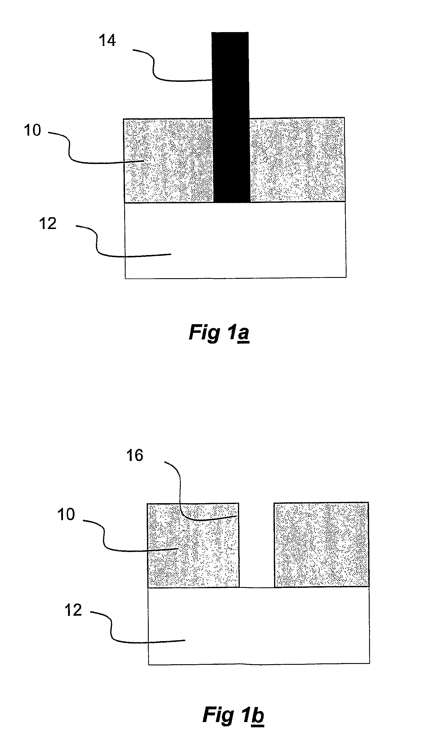
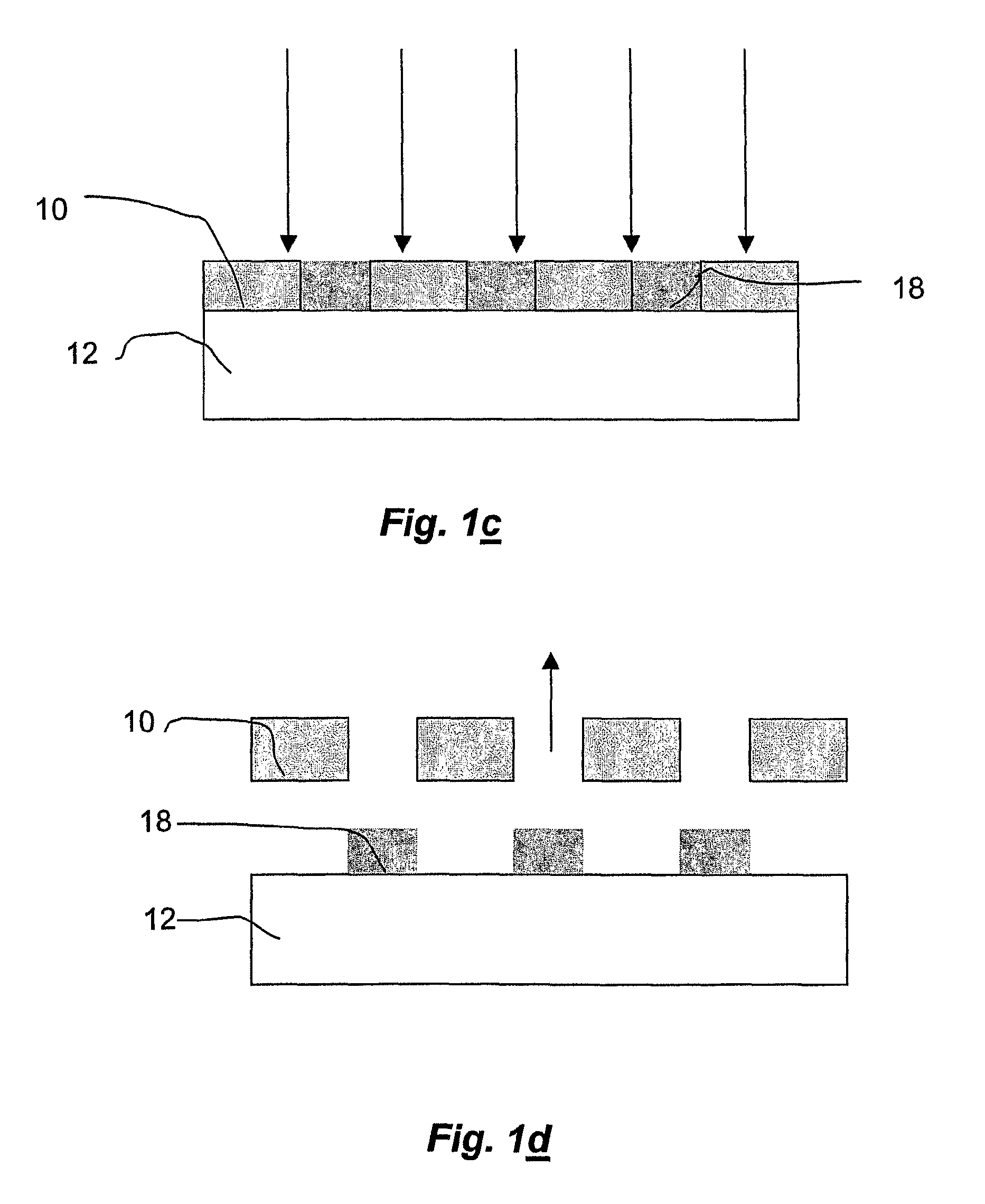
[0226]FIG. 1 shows schematically a number of stages in an embodiment of a process using a peelable mask. A peelable mask 10 which is a thin polymer film, for example a polyethylene terathalate, a polypropylene, a polyethylene napthalate, a polyethersulphone, or a polyimide, is laminated to a substrate 12, for example a glass material or a plastic material. The material may be rigid or conformable. The peelable mask 10 is laminated, or sprayed onto the substrate 12 and held thereon by electrostatic attraction and weak mechanical interlocking. Such a masking film can have a wide ranging selectable cross-sectional thickness in the range 0.1 to 200 μm, in this embodiment around 10 μm, that is preferably applied dry in sheet form for roll-to-roll or roll-to-substrate coverage applications. Some of the dry film polymers, such as 0.9 micron thick PET can be obtained in 4 meter wide rolls thereby providing for very large area array processing.

[0227]Alternatively the ...

example

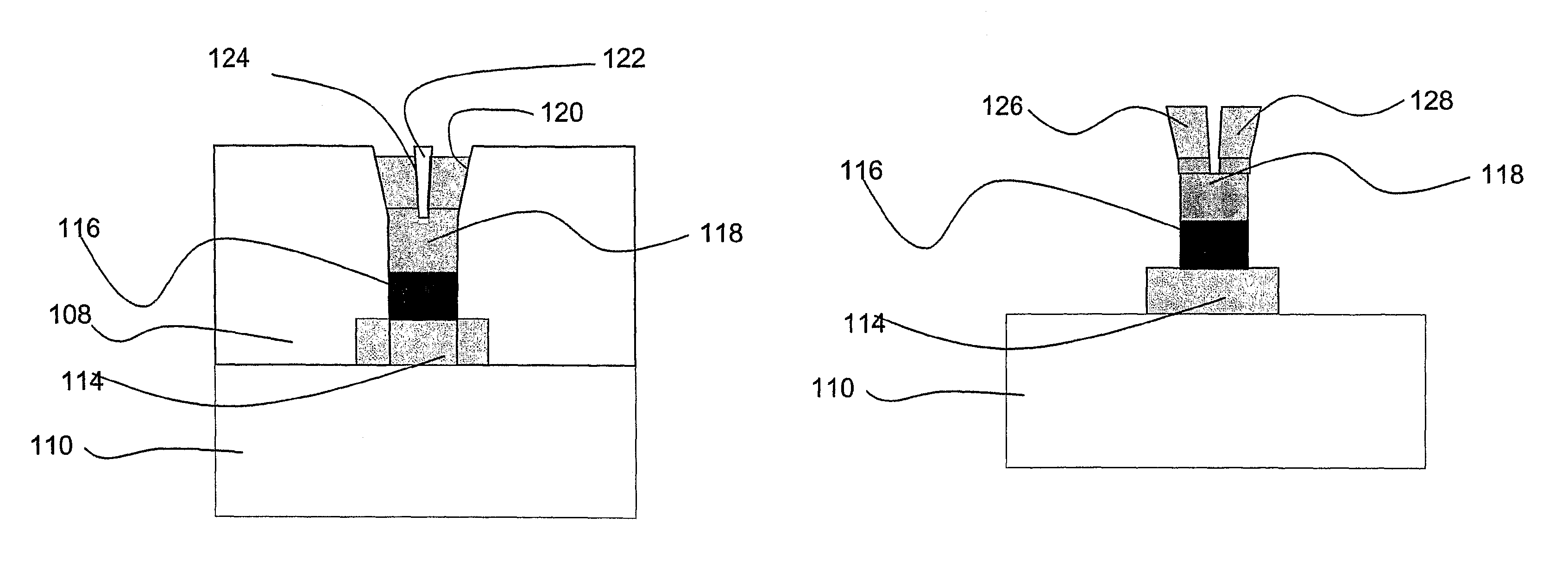
[0499]FIG. 51 shows a single pixel circuit 790 that can be used to switch a high (for this illustration 60 volts but in principle even very high voltages exceeding 200 volts can be supported) voltage liquid crystal display element. The device shown in this illustration is able to switch a high voltage without degrading the transistor performance. Since the transistor switching circuit is transparent it is possible to provide a solution that makes use of a number of thin film transistors that are switched in unison (all at once), using a common connected gate 792 and interlinked drain 794 and source 796 electrodes are shown in FIG. 49.

[0500]An alternative device is shown in FIG. 50. FIG. 50a shows a device 800 before removal of the mask; and FIG. 50b shows the device 800 after the removal of the mask. The device comprises a drain and source contact wells 802, 804 a plurality of interdigitated interlinked gate electrodes 806, the electrodes 806 are interdigitated with an insulator and...


PUM

PropertyMeasurementUnit
thicknessaaaaaaaaaa
thicknessaaaaaaaaaa
thicknessaaaaaaaaaa

Abstract

A method of manufacturing microstructures is disclosed, the method comprising a applying a mask to substrate; forming a pattern in the mask; processing the substrate according to the pattern; and mechanically removing the mask from the substrate. A polymer mask is disclosed for manufacturing micro scale structure, the polymer mask comprising a thin, preferably ultra thin flexible film. A method of manufacturing an integrated circuit is disclosed, the method comprising forming a plurality of isolated semiconductor devices on a common substrate; and connecting some of the devices. Apparatus for manufacturing microstructures is disclosed comprising: a mechanism for coating a mass substrate to create a structure; a mechanism for removing a mask from the substrate; and processing apparatus. A thin film transistor is disclosed comprising drain source and gate electrodes, the drain and source electrode being separated by a semiconductor, and the gate electrode being separated from the semiconductor by an insulator, comprising a bandgap alignment layer disposed between a semiconductor and the insulator.

Description

CROSS-REFERENCE TO OTHER APPLICATIONS[0001]This is a National Phase of International Application No. PCT / GB2006 / 001468, filed on Apr. 21, 2006, which claims priority from Great Britain Patent Application No. 0508101.3, filed on Apr. 21, 2005 and Great Britain Patent Application No. 0511976.3, filed on Jun. 13, 2005.BACKGROUND OF THE INVENTION[0002]This invention relates to methods and apparatus for the manufacture of microstructures. In particular, but not exclusively, this invention relates to the methods and apparatus for the manufacturer of semiconductor devices, and other microstructures, such methods involving the use of masking techniques. This invention also relates to novel microstructures, in particular, but not exclusively, novel semiconductor devices particularly those which may be manufactured by the use of masking techniques. This invention is of particular, although not exclusive, relevance to the field of thin film transistors, particularly transparent thin film trans...

Claims


Application Information

Patent Timeline
Patent Type & Authority Patents(United States)
IPC IPC(8): G03F7/26G03F1/00G03F7/34H01L21/336H01L21/77H01L29/49H01L29/786H05K3/00H05K3/06
CPCG03F1/56G03F1/68G03F7/343G03F7/346H01L27/1288H01L27/1292H01L29/4908H01L29/66757H01L29/78603H01L29/78645H01L29/7869H05K3/0079H05K3/0032H05K3/061H05K2203/107G03F7/26
Inventor SPEAKMAN, STUART PHILIP
Owner 3T TECH
Why Eureka
Try Eureka